CY7C1482V33-200BZXC(2004) データシートの表示(PDF) - Cypress Semiconductor
部品番号
コンポーネント説明
メーカー
CY7C1482V33-200BZXC
(Rev.:2004)
(Rev.:2004)
Cypress Semiconductor

CY7C1482V33-200BZXC Datasheet PDF : 30 Pages
| |||
PRELIMINARY
CY7C1480V33
CY7C1482V33
CY7C1486V33
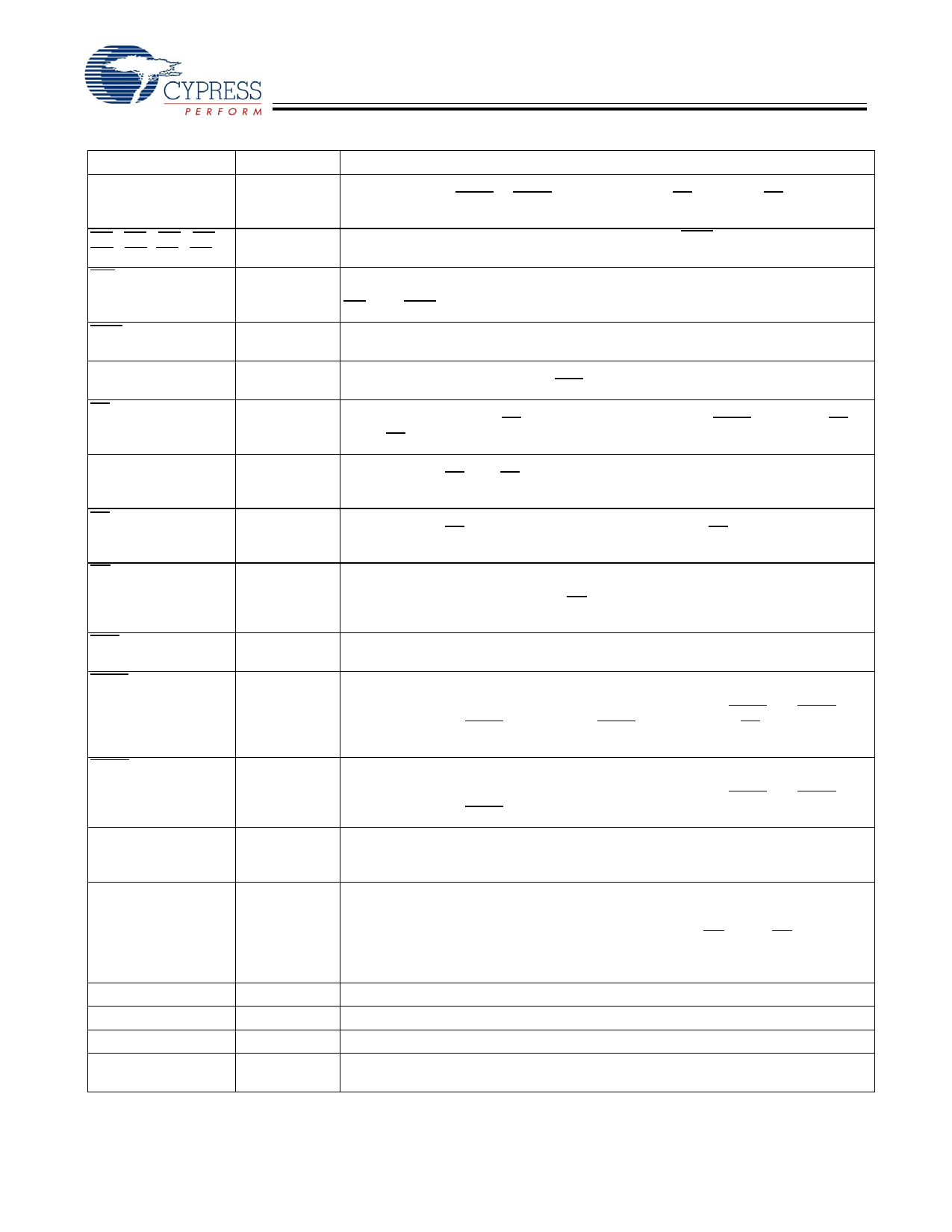
Pin Definitions
Pin Name
A0, A1, A
BWA,BWB,BWC,BWD,
BWE,BWF,BWG,BWH
GW
BWE
CLK
CE1
CE2
CE3
OE
ADV
ADSP
ADSC
ZZ
DQs, DQPs
VDD
VSS
VSSQ
VDDQ
MODE
I/O
Description
Input-
Address Inputs used to select one of the address locations. Sampled at the rising
Synchronous edge of the CLK if ADSP or ADSC is active LOW, and CE1, CE2, and CE3 are sampled
active. A1: A0 are fed to the two-bit counter.
Input-
Byte Write Select Inputs, active LOW. Qualified with BWE to conduct byte writes to
Synchronous the SRAM. Sampled on the rising edge of CLK.
Input-
Synchronous
Input-
Synchronous
Global Write Enable Input, active LOW. When asserted LOW on the rising edge of
CLK, a global write is conducted (ALL bytes are written, regardless of the values on
BWX and BWE).
Byte Write Enable Input, active LOW. Sampled on the rising edge of CLK. This signal
must be asserted LOW to conduct a byte write.
Input-
Clock
Clock Input. Used to capture all synchronous inputs to the device. Also used to
increment the burst counter when ADV is asserted LOW, during a burst operation.
Input-
Chip Enable 1 Input, active LOW. Sampled on the rising edge of CLK. Used in
Synchronous conjunction with CE2 and CE3 to select/deselect the device. ADSP is ignored if CE1 is
HIGH.
Input-
Chip Enable 2 Input, active HIGH. Sampled on the rising edge of CLK. Used in
Synchronous conjunction with CE1 and CE3 to select/deselect the device.
Input-
Chip Enable 3 Input, active LOW. Sampled on the rising edge of CLK. Used in
Synchronous conjunction with CE1 and CE2 to select/deselect the device.
Input-
Output Enable, asynchronous input, active LOW. Controls the direction of the I/O
Asynchronous pins. When LOW, the I/O pins behave as outputs. When deasserted HIGH, I/O pins are
tri-stated, and act as input data pins. OE is masked during the first clock of a read cycle
when emerging from a deselected state.
Input-
Advance Input signal, sampled on the rising edge of CLK, active LOW. When
Synchronous asserted, it automatically increments the address in a burst cycle.
Input-
Synchronous
Address Strobe from Processor, sampled on the rising edge of CLK, active LOW.
When asserted LOW, addresses presented to the device are captured in the address
registers. A1: A0 are also loaded into the burst counter. When ADSP and ADSC are
both asserted, only ADSP is recognized. ASDP is ignored when CE1 is deasserted
HIGH.
Input-
Synchronous
Address Strobe from Controller, sampled on the rising edge of CLK, active LOW.
When asserted LOW, addresses presented to the device are captured in the address
registers. A1: A0 are also loaded into the burst counter. When ADSP and ADSC are
both asserted, only ADSP is recognized.
Input-
ZZ “sleep” Input, active HIGH. When asserted HIGH places the device in a
Asynchronous non-time-critical “sleep” condition with data integrity preserved. For normal operation,
this pin has to be LOW or left floating. ZZ pin has an internal pull-down.
I/O-
Synchronous
Bidirectional Data I/O lines. As inputs, they feed into an on-chip data register that is
triggered by the rising edge of CLK. As outputs, they deliver the data contained in the
memory location specified by the addresses presented during the previous clock rise
of the read cycle. The direction of the pins is controlled by OE. When OE is asserted
LOW, the pins behave as outputs. When HIGH, DQs and DQPX are placed in a tri-state
condition.
Power Supply Power supply inputs to the core of the device.
Ground Ground for the core of the device.
I/O Ground Ground for the I/O circuitry.
I/O Power Power supply for the I/O circuitry.
Supply
Input Static
Selects Burst Order. When tied to GND selects linear burst sequence. When tied to
VDD or left floating selects interleaved burst sequence. This is a strap pin and should
remain static during device operation. Mode Pin has an internal pull-up.
Document #: 38-05283 Rev. *C
Page 7 of 30
Share Link: