CY7C1482BV25-200BZXC データシートの表示(PDF) - Cypress Semiconductor
部品番号
コンポーネント説明
メーカー
CY7C1482BV25-200BZXC Datasheet PDF : 31 Pages
| |||
CY7C1480BV25
CY7C1482BV25, CY7C1486BV25
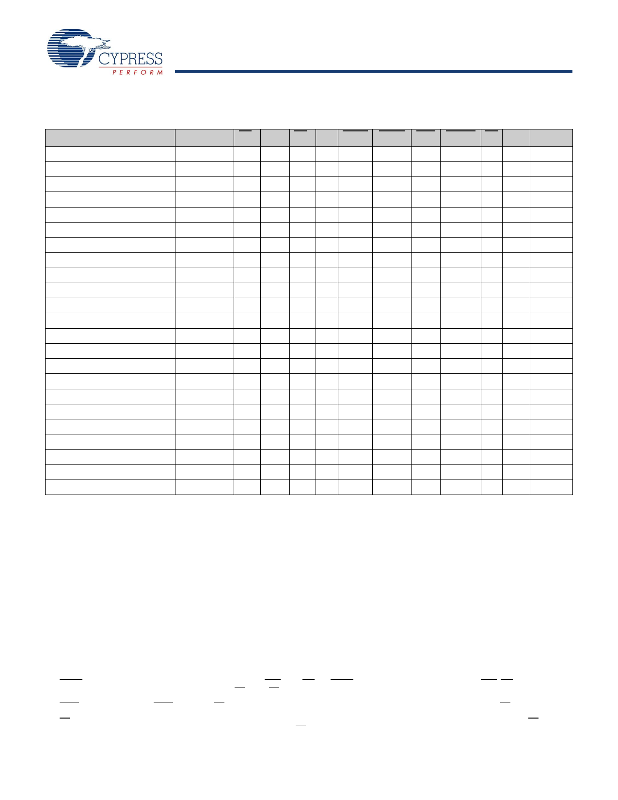
Table 4. Truth Table
The truth table for CY7C1480BV25, CY7C1482BV25, and CY7C1486BV25 follows.[3, 4, 5, 6, 7]
Operation
Deselect Cycle, Power Down
Deselect Cycle, Power Down
Deselect Cycle, Power Down
Deselect Cycle, Power Down
Deselect Cycle, Power Down
Sleep Mode, Power Down
Read Cycle, Begin Burst
Read Cycle, Begin Burst
Write Cycle, Begin Burst
Read Cycle, Begin Burst
Read Cycle, Begin Burst
Read Cycle, Continue Burst
Read Cycle, Continue Burst
Read Cycle, Continue Burst
Read Cycle, Continue Burst
Write Cycle, Continue Burst
Write Cycle, Continue Burst
Read Cycle, Suspend Burst
Read Cycle, Suspend Burst
Read Cycle, Suspend Burst
Read Cycle, Suspend Burst
Write Cycle, Suspend Burst
Write Cycle, Suspend Burst
Add. Used CE1 CE2 CE3 ZZ ADSP ADSC ADV WRITE OE CLK DQ
None
H X XL X
L
X
X
X L-H Tri-State
None
L
L
XL
L
X
X
X
X L-H Tri-State
None
L
X HL
L
X
X
X
X L-H Tri-State
None
L L XL H
L
X
X
X L-H Tri-State
None
L X HL H
L
X
X
X L-H Tri-State
None
X X XH X
X
X
X
X X Tri-State
External
L
H
LL
L
X
X
X
L L-H
Q
External
L
H
LL
L
X
X
X
H L-H Tri-State
External
L
H
LL
H
L
X
L
X L-H
D
External
L
H
LL
H
L
X
H
L L-H
Q
External
L
H
LL
H
L
X
H
H L-H Tri-State
Next
X X XL H
H
L
H
L L-H
Q
Next
X X XL H
H
L
H
H L-H Tri-State
Next
H X XL X
H
L
H
L L-H
Q
Next
H X XL X
H
L
H
H L-H Tri-State
Next
X X XL H
H
L
L
X L-H
D
Next
H X XL X
H
L
L
X L-H
D
Current
X X XL H
H
H
H
L L-H
Q
Current
X X XL H
H
H
H
H L-H Tri-State
Current
H X XL
X
H
H
H
L L-H
Q
Current
H X XL
X
H
H
H
H L-H Tri-State
Current
X X XL H
H
H
L
X L-H
D
Current
H X XL X
H
H
L
X L-H
D
Notes
3. X = Do Not Care, H = Logic HIGH, L = Logic LOW.
4. WRITE = L when any one or more Byte Write Enable signals and BWE = L or GW = L. WRITE = H when all Byte Write Enable signals, BWE, GW = H.
5. The DQ pins are controlled by the current cycle and the OE signal. OE is asynchronous and is not sampled with the clock.
6. The SRAM always initiates a read cycle when ADSP is asserted, regardless of the state of GW, BWE, or BWX. Writes may occur only on subsequent clocks after the
ADSP or with the assertion of ADSC. As a result, OE must be driven HIGH before the start of the write cycle to enable the outputs to tri-state. OE is a do not care for
the remainder of the write cycle
7. OE is asynchronous and is not sampled with the clock rise. It is masked internally during write cycles. During a read cycle all data bits are tri-state when OE is inactive
or when the device is deselected, and all data bits behave as outputs when OE is active (LOW).
Document #: 001-15143 Rev. *D
Page 10 of 31
[+] Feedback
Share Link: 