1DDD356AA-K01 データシートの表示(PDF) - Unspecified
部品番号
コンポーネント説明
メーカー
1DDD356AA-K01 Datasheet PDF : 12 Pages
| |||
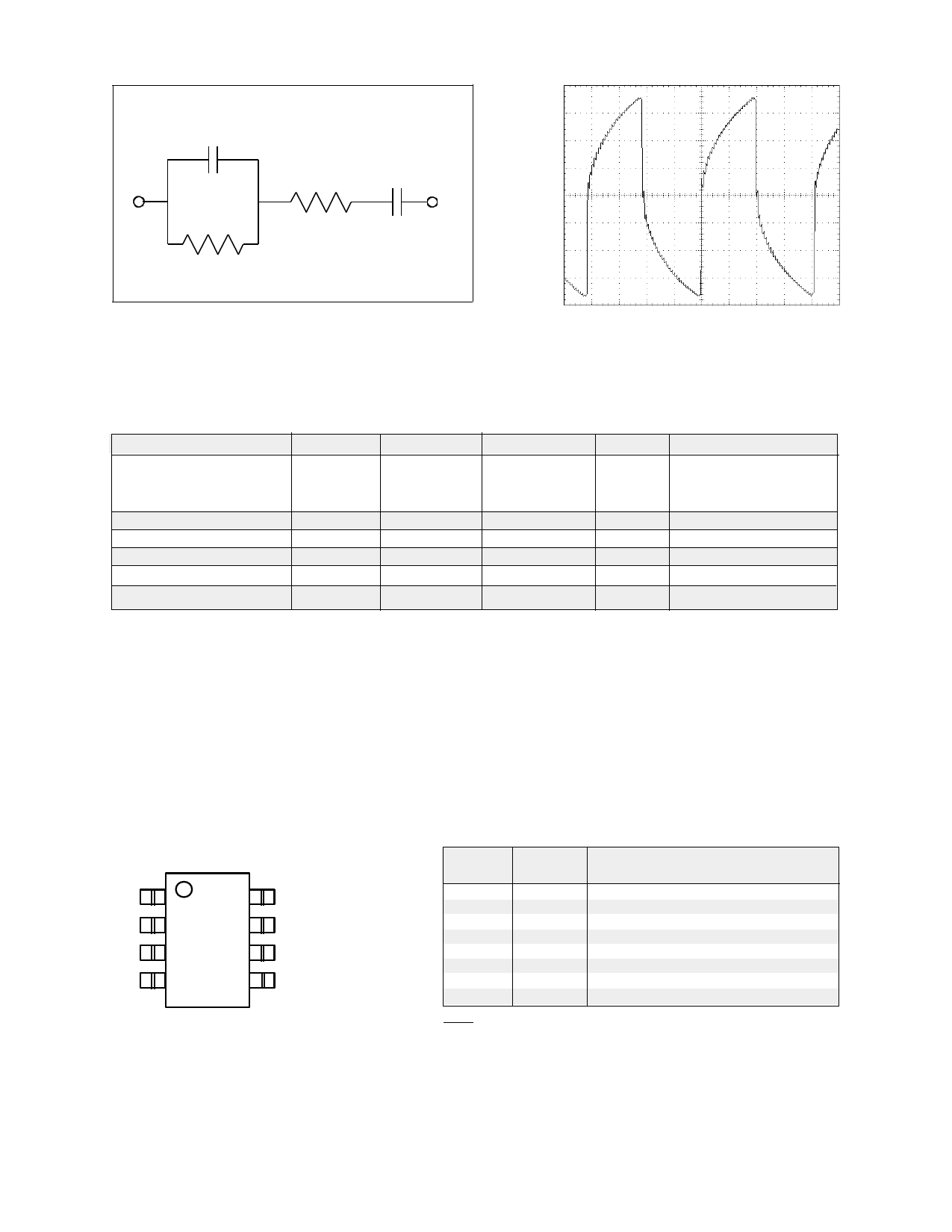
Load B*
47 nF
10kW
100W 22 nF
Typical Output Waveform
* Load B approximates a 5in2 EL lamp.
Absolute Maximum Ratings:
Parameter
Supply voltage
Operating Range
Withstand Range
Enable Voltage
Output Voltage
CLF Voltage
Operating Temperature
Storage Temperature
Symbol
V+
E
VOUT
VCLF
Ta
Ts
Minimum Maximum
1.0
7.0
-0.5
10.0
-0.5
(V+) +0.5
220
0
(V+) +0.3
-40
85
-65
150
Unit
V
V
Vpp
V
°C
°C
Comments
E = V+
E = GND
Peak-to-peak voltage
External clock input
Note: The above are stress ratings only. Functional operation of the device at these ratings or any other above
those indicated in the specifications is not implied. Exposure to absolute maximum rating conditions for extended
periods of time may affect reliability.
Physical Data:
1
8
2
7
3
6
4
5
PIN # NAME
FUNCTION
1
GND System ground connection
2
L-
Negative input to inductor
3
VOUT High voltage AC output to lamp
4
L+
Positive input to inductor
5
V+
DC power supply input
6
CLF1 Lamp frequency capacitor/clock input
7
CLF2 Lamp frequency capacitor/clock input
8
E
System enable
Note: Please consult factory for bare die dimensions and bond
pad locations.
2
Share Link: 