ES636_09 データシートの表示(PDF) - Cyrustek corporation
部品番号
コンポーネント説明
メーカー
ES636_09 Datasheet PDF : 13 Pages
| |||
ES636
True RMS-to-DC Converters
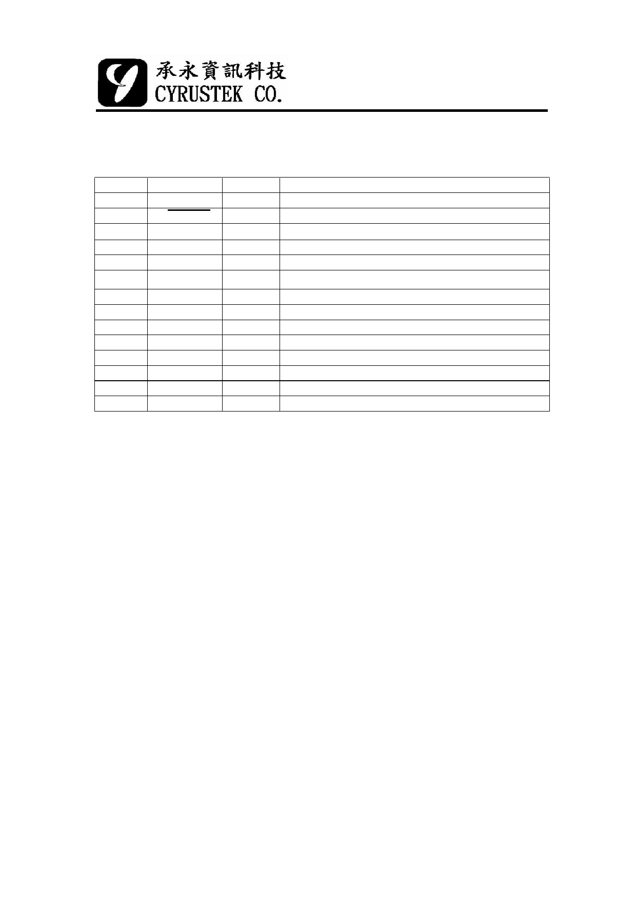
Pin Description
Pin No
1
2
3
4
5
6
7
8
9
10
11
12
13
14
Symbol
Vin
Enable
-Vs
Cav
dB
BUF OUT
BUF IN
Iout
RL
COMMON
N.C.
N.C.
N.C
+Vs
Type
I
I
P
IO
IO
O
I
O
IO
G
Description
Measurement input
Chip enable, active LOW
Negative supply voltage
Averaging capacitor
DB out
Buffer output
Buffer input
Rms output
RL terminal, connected to COMMON in general
Analog ground
P Positive supply voltage
Absolute Maximum Ratings
Supply Voltage: Dual Supplies ......…………………………….….... ±10V
Single Supply ..……………………...…….....……+20V
Input Voltage: ...................………………………….……………..... ±10V
Power Dissipation (Package)
SOP………………………………………………………………...450mW
Operating Temperature Range .......……………………………….......0℃ to +70℃
Storage Temperature Range.....…………………...……………............-55℃ to +150℃
Lead Temperature (Soldering, 10sec)....…………………………………...............300℃
3
09/02/16
Share Link: 