IA6805E2-PDW40I-00 データシートの表示(PDF) - InnovASIC, Inc
部品番号
コンポーネント説明
メーカー
IA6805E2-PDW40I-00 Datasheet PDF : 33 Pages
| |||
IA6805E2
Microprocessor Unit
As of Production Version 00
29 August 2007
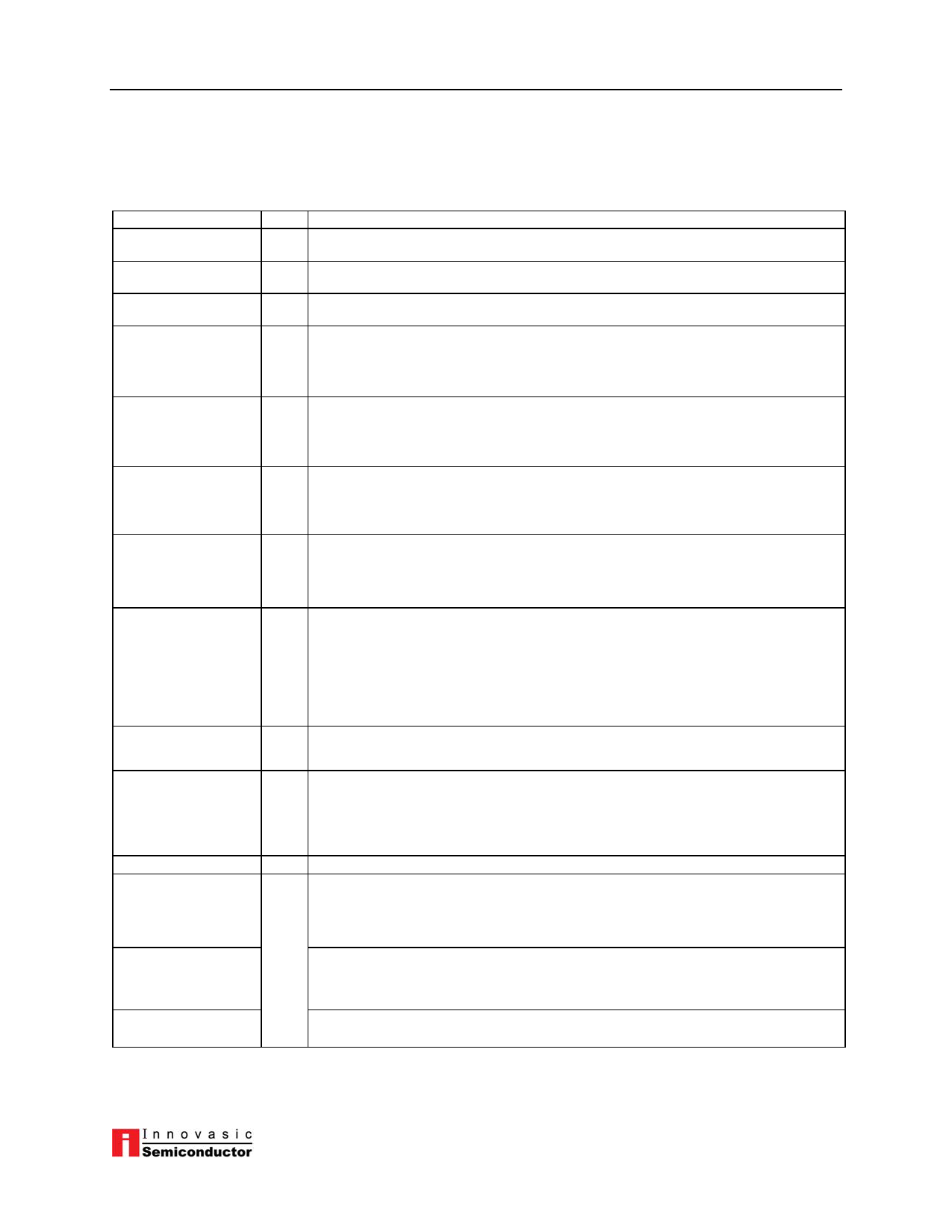
I/O Signal Description
The table below describes the I/O characteristics for each signal on the IC. The signal names
correspond to the signal names on the pinout diagrams provided.
SIG N AL NAM E
VDD and VSS
(Pow er and G round)
RESET_n
(R e s e t)
IR Q _n
(Interrupt Request)
LI
(Load Instruction)
I/O D ESC R IPT IO N
N /A
S o u rce: T hese tw o pins provide pow er to the chip. V DD provides +5 volts (±0.5)
pow er and V SS is ground.
T T L : Input pin that can be used to reset the M P U 's internal state by pulling the reset_n
I pin low .
T T L : Input pin that is level and edge sensitive. C an be used to request an interrupt
I sequence.
T T L w ith slew rate co n tro l: O utput pin used to indicate that a next opcode fetch is in
progress. U sed only for certain debugging and test system s. N ot connected in
O norm al operation. O verlaps D ata S trobe (D S ) signal. T his output is capable of driving
one standard T T L load and 50pF .
DS
(Data Strobe)
RW _n
(R ead/W rite)
AS
(Address Strobe)
PA0-PA7/PB 0-PB 7
(Input/O utput Lines)
T T L w ith slew rate co n trol: O utput pin used to transfer data to or from a peripheral
or m em ory. D S occurs anytim e the M P U does a data read or w rite and during data
O transfer to or from internal m em ory. D S is available at fOSC ¸5 w hen the M P U is not in
the W A IT or S T O P m ode. T his output is capable of driving one standard T T L load and
130pF.
T T L w ith slew rate co n tro l: O utput pin used to indicate the direction of data transfer
from internal m em ory, I/O registers, and external peripheral devices and m em ories.
O Indicates to a selected peripheral w hether the M P U is to read (R W _n high) or w rite
(R W _n low ) data on the next data strobe. T his output is capable of driving one
standard T T L load and 130pF .
T T L w ith slew rate co n trol: O utput strobe used to indicate the presence of an
address on the 8-bit m ultiplexed bus. T he A S line is used to dem ultiplex the eight
O least significant address bits from the data bus. A S is available at fOSC ¸ 5 w hen the
M P U is not in the W A IT or S T O P m odes. T his output is capable of driving one
standard T T L load and 130pF .
T T L w ith slew rate co ntro l: T hese 16 lines constitute Input/O utput ports A and B .
E ach line is individually program m ed to be either an input or output under softw are
control of the D ata D irection R egister (D D R ) as show n below in T ab le 1 and F igu re 2.
T he port I/O is program m ed by w riting the corresponding bit in the D D R to a "1" for
I/O output and a "0" for input. In the output m ode the bits are latched and appear on the
corresponding output pins. A ll the D D R 's are initialized to a "0" on reset. T he output
port registers are not initialized on reset. E ach output is capable of driving one
standard T T L load and 50pF .
A8-A12
T T L w ith slew rate control: T hese five outputs constitute the higher order non-
(High O rder Address
L in e s )
O m ultiplexed address lines. E ach output is capable of driving one standard T T L load
and 130pF.
B 0 -B 7
(Address/D ata B us)
T T L w ith slew rate con tro l: T hese bi-directional lines constitute the low er order
addresses and data. T hese lines are m ultiplexed w ith address present at address
I/O
strobe tim e and data present at data strobe tim e. W hen in the data m ode, these lines
are bi-directional, transferring data to and from m em ory and peripheral devices as
indicated by the R W _n pin. A s outputs, these lines are capable of driving one
Tim er
standard T T L load and 130pF .
I T T L : Input used to control the internal tim er/counter circuitry.
T T L O scillator in p u t/o u tp u t: T hese pins provide control input for the on-chip clock
OSC1, OSC2
(System C lock)
oscillator circuits. E ither a crystal or external clock is connected to these pins to
provide a system clock. T he crystal connection is show n in Fig ure 3. T he O S C 1 to
bus transitions for system designs using oscillators slow er than 5M H z is show n in
Figure 4.
I/O T he circuit show n in F igu re 3 is recom m ended w hen using a crystal. A n external
C M O S oscillator is recom m ended w hen using crystals outside the specified ranges.
C rystal
T o m inim ize output distortion and start-up stabilization tim e, the crystal and
com ponents should be m ounted as close to the input pins as possible.
External C lock
W hen an external clock is used, it should be applied to the O S C 1 input w ith the O S C 2
input not connected, as show n in F ig ure 3.
Table 1
Copyright © 2007
©
IA211081401-03
Page 4 of 33
www.Innovasic.com
Customer Support:
1-888-824-4184
Share Link: 