IX2R11P7 データシートの表示(PDF) - IXYS CORPORATION
部品番号
コンポーネント説明
メーカー
IX2R11P7 Datasheet PDF : 6 Pages
| |||
IX2R11
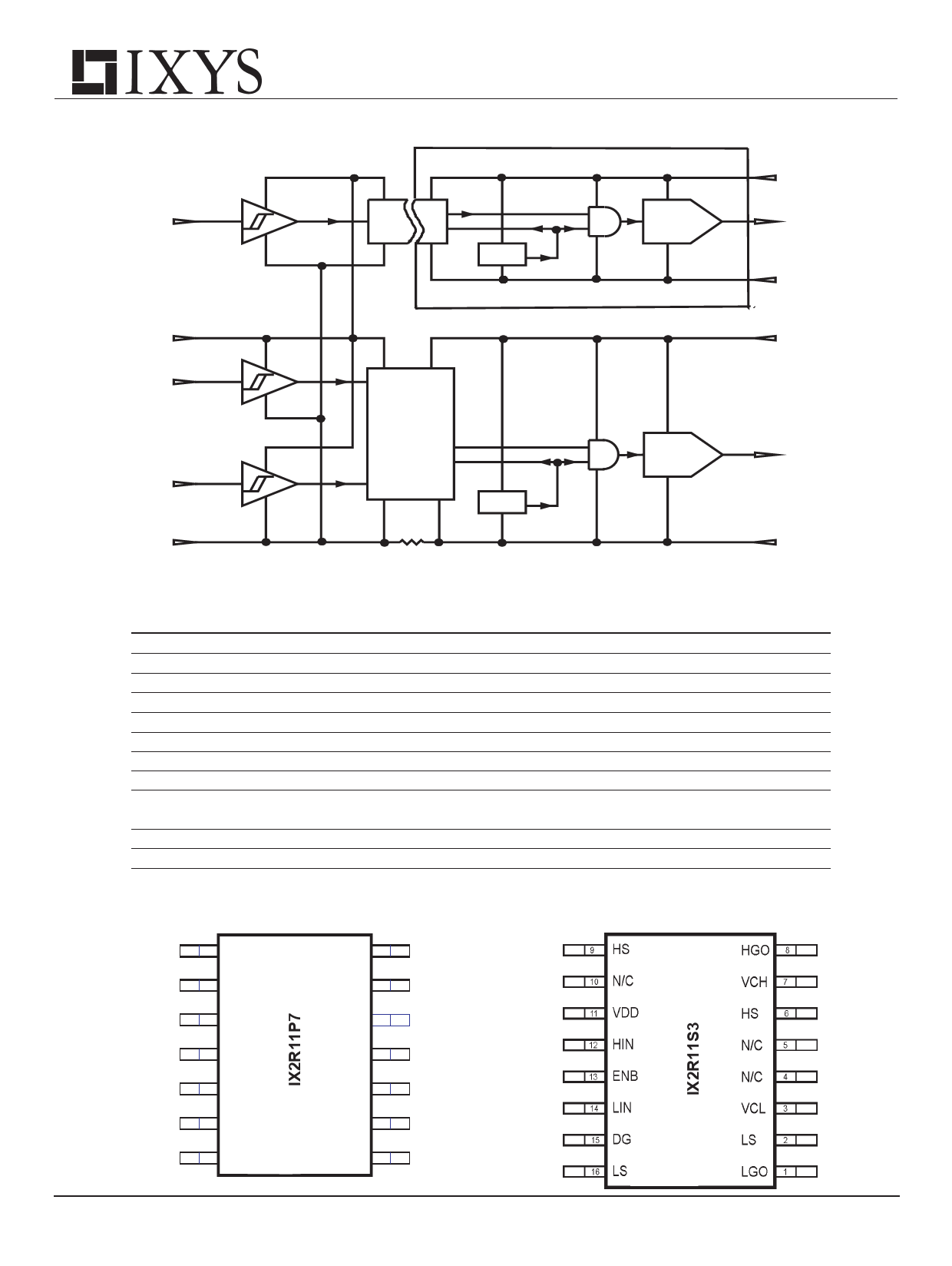
Figure 2 - IX2R11 Functional Block Diagram
VDD
Low to High
HIN
HIN
OUT
HIN
RST
IN
DG
VDD
VCH
UVCC
Detect
Gate Current
Output
HS
Isolated High Side
VCL
VCH
HGO
HS
VCL
LIN
ENB
DG
Low to High
Side Delay
Equalizer
and
Shutdown
Shutdown
Logic
DG
1 Ohm
UVCC
Detect
LS
Gate Current
Output
LGO
LS
Pin Description And Configuration
SYMBOL
VDD
HIN
LIN
ENB
DG
VCH
HGO
HS
VCL
FUNCTION
Logic Supply
HS Input
LS Input
Not Enable
Ground
Supply Voltage
Output
Return
Supply Voltage
LGO
LS
Output
Ground
DESCRIPTION
Positive power supply for the chip CMOS functions
High side Input signal, TTL or CMOS compatible; HGO in phase
Low side Input signal, TTL or CMOS compatible; LGO in phase
Chip enable. When driven high, both outputs go low.
Logic Reference Ground
High Side Power Supply
High side driver output
High side voltage return pin
Low side power supply. This power supply provides power for
both outputs. Voltage range is from 4.5 to 25V.
Low side driver output
Low side return
14-PIN DIP
8 N/C
9 VDD
10 HIN
11 ENB
12 LIN
13 DG
14 NC
HGO 7
VCH 6
HS 5
N/C 4
VCL 3
LS 2
LGO 1
16-PIN SOIC
2
Share Link: 