IX2R11S3 データシートの表示(PDF) - IXYS CORPORATION
部品番号
コンポーネント説明
メーカー
IX2R11S3 Datasheet PDF : 6 Pages
| |||
Dynamic Electrical Characteristics
Symbol Definition
Test Conditions
Min
ton
Turn-on propagation delay
VHS= 0V, Cload= 2nF
toff
Turn-off propagation delay
VHS= 600V, Cload= 2nF
tenb
Device Not enable delay
tr
Turn-on rise time
Cload= 2nF
tf
Turn-off fall time
Cload= 2nF
tdm
Delay matching, HS & LS turn-on/off Cload= 2nF
Static Electrical Characteristics
Symbol Definition
Test Conditions
Min
VINH
Logic “1” input voltage
VDD= VCL= 15V
7.0
VINL
Logic “0” input voltage
VHLGO // VHHGO High level output voltage,
VCH-VHGO or VCL-VLGO
VLLGO // VLHGO High level output voltage,
VHGO or VLGO
IHL
HS to LS bias current.
VDD= VCC= 15V
IO= 0A
IO= 0A
VHS= VCH= 600V
IQHS
Quiescent VCH supply current
VIN= 0V or VDD
IQLS
Quiescent VCL supply current
VIN= 0V or VDD
IQDD
Quiescent VDD supply current
VIN= 0V or VDD
IIN+
Logic “1” input bias current
VIN= VDD
IIN-
VCHUV+
Logic “0” input voltage
VIN= 0V
VCH supply undervoltage positive going threshold.
VCHUV-
VCLUV+
VCLUV-
IGO+
IGO-
VCH supply undervoltage negative going threshold.
VCL supply undervoltage positive going threshold
VCL supply undervoltage negative going threshold.
HS or LS Output low short circuit current; VGO= 15V, VIN= 0V, PW<10us +2
HS or LS Output low short circuit current; VGO= 15V, VIN=0V, PW<10us
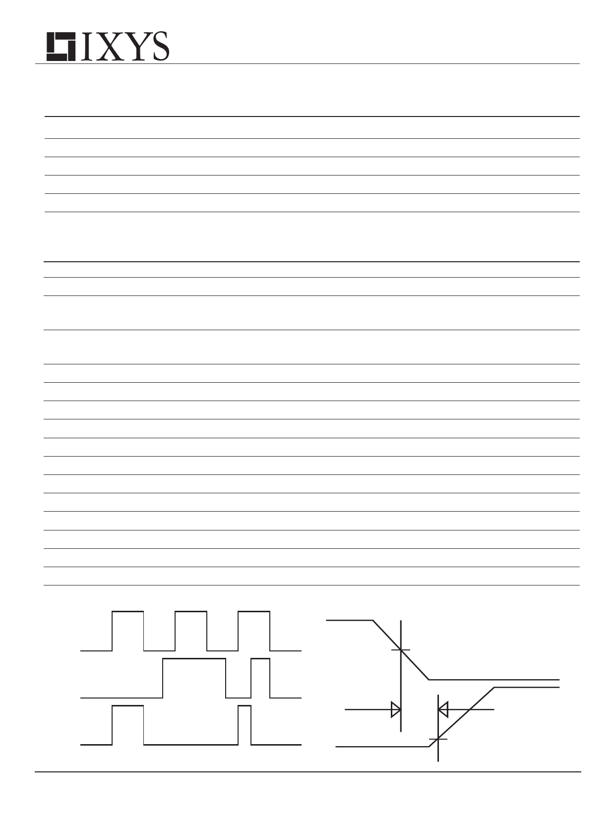
Timing Waveform Definitions
ENB
HIN/LIN
50%
IX2R11
Typ Max Units
120
ns
87
ns
202
ns
23
ns
22
ns
10
20
ns
Typ Max Units
V
6
V
0.28
V
.23
V
.17
mA
.77
mA
.79
mA
36
uA
2
uA
1
uA
8.3
V
8.2
V
8.1
V
8.0
V
A
-2
A
ENB
LGO/HGO
Figure 3. INPUT/OUPUT Timing Diagram
tenb
LGO/HGO
10%
Figure 4. ENABLE Waveform Definitions
4
Share Link: 