MAX6575L データシートの表示(PDF) - Maxim Integrated
部品番号
コンポーネント説明
メーカー
MAX6575L Datasheet PDF : 12 Pages
| |||
SOT Temperature Sensor with
Multidrop Single-Wire Digital Interface
_______________Detailed Description
The MAX6575L/H low-cost, low-current (150µA typ)
temperature sensor is ideal for interfacing with micro-
controllers or microprocessors. The MAX6575L/H is a
monostable, externally triggered temperature sensor
that uses a Temp→Delay conversion to communicate
with a µP over a single I/O line. Time-select pins (TS1,
TS0) permit the internal temperature-controlled oscilla-
tor (TCO) to be scaled by four preset timeout multipli-
ers, allowing eight separate temperature sensors to
share one I/O line. Different sensors on the same I/O
line will use different timeout multipliers to avoid over-
lapping signals.
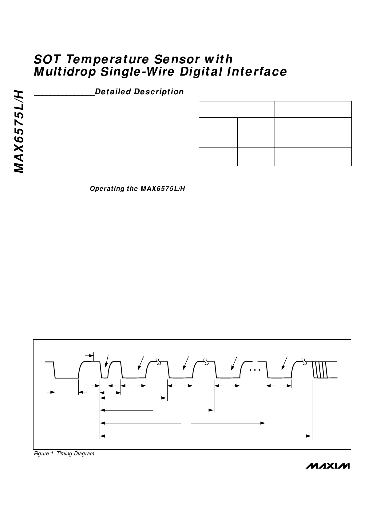
Operating the MAX6575L/H
Figure 1 illustrates the timing for the MAX6575L/H.
When the device is powered up, it assumes a ready
state where it awaits an external trigger at the I/O pin.
The I/O pin of the MAX6575L/H has an open-drain out-
put structure that requires a pull-up resistor to maintain
the proper logic levels. Once the I/O pin is pulled low
and then released, control of the I/O pin is transferred
to the MAX6575L/H. The temperature conversion
begins on the falling edge of the externally triggered
pulse. The I/O line is pulled low at a later time. That time
is determined by the device temperature and the Time
Select pins (TS1, TS0). The I/O line remains low for
5Tµs, where T is the temperature in degrees Kelvin. The
temperature of the device is represented by the edge-
to-edge delay of the externally triggered pulse and the
falling edge of the subsequent pulse originating from
the device. The device can be manually reset by
pulling the I/O line low for more than tRESET (16ms
max). The device will automatically reset after a maxi-
Table 1. Time-Select Pin Configuration
TIME-SELECT PINS
TS1
GND
GND
VDD
VDD
TS0
GND
VDD
GND
VDD
TIMEOUT MULTIPLIERS
(µs/°K)
MAX6575L MAX6575H
5
160
20
320
40
480
80
640
mum delay of 520ms, at which point it will again be in a
ready state awaiting a start pulse.
Definition of Terms:
tRESET: Time I/O must be externally pulled low to guar-
antee the MAX6575L/H is in a ready state
awaiting external trigger. (Part will assume a
ready state after 520ms without a reset pulse.)
tSETUP: Time I/O must be high prior to a start pulse.
tSTART: Trigger pulse which starts the on-chip timing
sequence on its falling edge.
tDx: Timing delay between the falling edge of the
start pulse and the falling edge initiated by
CHIP#x.
tLx: I/O pulse low time (5Tµs).
tREADY: Time after falling edge of start pulse when the
MAX6575L/H will reset itself and await the next
external trigger.
The temperature, in degrees Celsius, may be calculat-
ed as follows:
T(°C) = [tDx(µs) / timeout multiplier(µs/°K)] - 273.15°K
tSETUP
APPLIED START CHIP# 1
PULSE
RESPONSE
CHIP# 2
RESPONSE
CHIP# 3
RESPONSE
CHIP# 4
RESPONSE
tSTART
tL1
tL2
tL3
tL4
tRESET
tD1
tD2
tD3
tD4
tREADY
Figure 1. Timing Diagram
4 _______________________________________________________________________________________
Share Link: 