MAX9685CSE データシートの表示(PDF) - Maxim Integrated
部品番号
コンポーネント説明
メーカー
MAX9685CSE Datasheet PDF : 8 Pages
| |||
Ultra-Fast ECL-Output Comparator
with Latch Enable
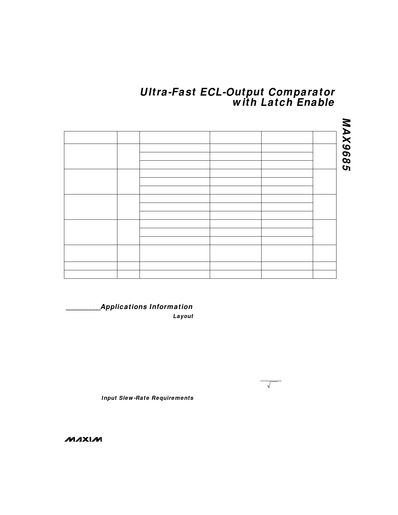
SWITCHING CHARACTERISTICS
(V+ = 5V, V- = -5.2V, RL = 50Ω, VT = -2V, TA = +25°C, unless otherwise noted.)
PARAMETER
SYMBOL
CONDITIONS
MAX9685C/E
MIN TYP MAX
Input to Output High
(Notes 1, 2)
TA = +25°C
tpd+ TA = 0°C to +70°C
TA = -55°C to +125°C
1.3 1.8
1.5 2.0
Input to Output Low
(Notes 1, 2)
TA = +25°C
tpd- TA = 0°C to +70°C
TA = -55°C to +125°C
1.3 1.8
1.5 2.0
Latch-Enable to Output
High (Notes 1, 2)
tpd+(E)
TA = +25°C
TA = 0°C to +70°C
TA = -55°C to +125°C
1.2 1.7
1.4 2.0
Latch-Enable to Output
High (Notes 1, 2)
tpd-(E)
TA = +25°C
TA = 0°C to +70°C
TA = -55°C to +125°C
1.2 1.7
1.4 2.0
Latch-Enable Pulse
Width (Note 2)
tpw(E)
3.0 2.0
Minimum Setup Time
ts
Minimum Hold Time
th
0.5 1.0
0.5 1.0
Note 1: Not tested, guaranteed by design.
Note 2: VIN = 100mV, VOD = 10mV
MAX9685M
MIN TYP MAX
1.3 1.8
1.7 2.4
1.3 1.8
1.7 2.4
1.2 1.7
2.0 3.0
1.2 1.7
2.0 3.0
UNITS
ns
ns
ns
ns
3.0 2.0
ns
0.5 1.0
ns
0.5 1.0
ns
__________Applications Information
Layout
Because of the MAX9685’s large gain-bandwidth char-
acteristic, special precautions need to be taken if its
high-speed capabilities are to be used. A PC board
with a ground plane is mandatory. Mount all decou-
pling capacitors as close to the power-supply pins as
possible, and process the ECL outputs in microstrip
fashion, consistent with the load termination of 50Ω to
120Ω. For low-impedance applications, microstrip lay-
out at the input may also be helpful. Pay close atten-
tion to the bandwidth of the decoupling and terminating
components. Chip components can be used to mini-
mize lead inductance. An unused LE pin must be con-
nected to ground.
Input Slew-Rate Requirements
As with all high-speed comparators, the high gain-
bandwidth product of these devices creates oscillation
problems when the input traverses through the linear
region. For clean switching without oscillation or steps
in the output waveform, the input must meet certain
minimum slew-rate requirements. The tendency of the
part to oscillate is a function of the layout and source
impedance of the circuit employed. Poor layout and
larger source impedance will increase the minimum
slew-rate requirement.
Figure 1 shows a high-speed receiver application with
50Ω input and output termination. With this configura-
tion, in which a ground plane and microstrip PC board
were used, the minimum slew rate for clean output
switching is 1.6V/µs. Sine-wave inputs imply a mini-
mum signal size of 360mVRMS at 500kHz and
90mVRMS at 4MHz.
Slew Rate
ERMS =
2 2nf
In many applications, the addition of regenerative feed-
back will assist the input signal through the linear
region, which will lower the minimum slew-rate require-
ment considerably. For example, with the addition of
positive feedback components Rf = 1kΩ and Cf =
10pF, the minimum slew-rate requirement can be
reduced by a factor of four.
_______________________________________________________________________________________ 3
Share Link: 