MAX9685CSE データシートの表示(PDF) - Maxim Integrated
部品番号
コンポーネント説明
メーカー
MAX9685CSE Datasheet PDF : 8 Pages
| |||
Ultra-Fast ECL-Output Comparator
with Latch Enable
50Ω
VIN
LE
50Ω
-2V
50Ω
Rf
Cf
50Ω
INPUT
20mV/div
OUTPUT
500mV/div 2ns/div
INPUT
OUTPUT
-0V
-0.9V
-1.7V
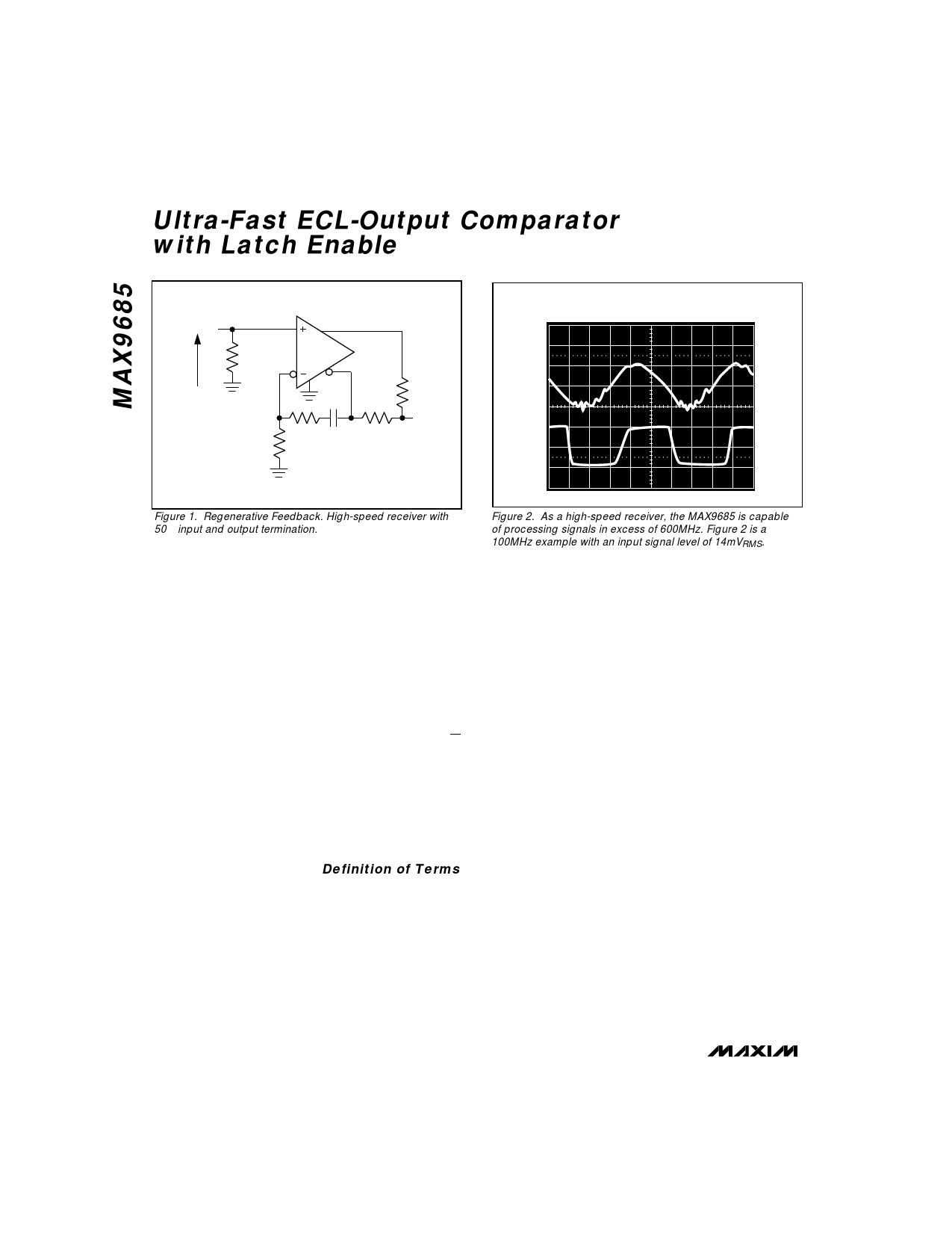
Figure 1. Regenerative Feedback. High-speed receiver with
50Ω input and output termination.
The timing diagram (Figure 3) illustrates the series of
events that complete the compare function, under
worst-case conditions.
The top line of the diagram illustrates two latch-enable
pulses. Each pulse is high for the compare function
and low for the latch function. The first pulse demon-
strates the compare function; part of the input action
takes place during the compare mode. The second
pulse demonstrates a compare-function interval during
which there is no change in the input.
The leading edge of the input signal (illustrated as a
large-amplitude, small-overdrive pulse) switches the
comparator after time interval tpd. Output Q and Q
transistors are similar in timing. The input signal must
occur at time ts before the latch falling edge, and it
must be maintained for time th after the edge to be
acquired. After th, the output is no longer affected by
the input status until the latch is again strobed. A mini-
mum latch pulse width of tpw(E) is needed for the
strobe operation, and the output transitions occur after
a time tpd(E).
Definition of Terms
VOS Input Offset Voltage—The voltage required
between the input terminals to obtain 0V dif-
ferential at the output.
VIN
Input Voltage Pulse Amplitude
VOD Input Voltage Overdrive
tpd+ Input to Output High Delay—The propagation
delay measured from the time the input signal
crosses the input offset voltage to the 50%
point of an output low-to-high transition.
Figure 2. As a high-speed receiver, the MAX9685 is capable
of processing signals in excess of 600MHz. Figure 2 is a
100MHz example with an input signal level of 14mVRMS.
tpd- Input to Output Low Delay—The propagation
delay measured from the time the input signal
crosses the input offset voltage to the 50%
point of an output high-to-low transition.
tpd+(E)
Latch-Enable to Output High Delay—The
propagation delay measured from the 50%
point of the latch-enable signal low-to-high
transition to the 50% point of an output low-to-
high transition.
tpd-(E)
Latch-Enable to Output Low Delay—The
propagation delay measured from the 50%
point of the latch-enable signal low-to-high
transition to the 50% point of an output high-
to-low transition.
tpw(E) Minimum Latch-Enable Pulse Width—The
minimum time the latch-enable signal must be
high to acquire and hold an input signal.
ts
Minimum Setup Time—The minimum time
before the negative transition of the latch-
enable pulse that an input signal must be pre-
sent to be acquired and held at the outputs.
th
Minimum Hold Time—The minimum time after
the negative transition of the latch-enable signal
that an input signal must remain unchanged to
be acquired and held at the output.
4 _______________________________________________________________________________________
Share Link: 