SD12 データシートの表示(PDF) - Microchip Technology
部品番号
コンポーネント説明
メーカー
SD12 Datasheet PDF : 38 Pages
| |||
MCP16301
3.0 PIN DESCRIPTIONS
The descriptions of the pins are listed in Table 3-1.
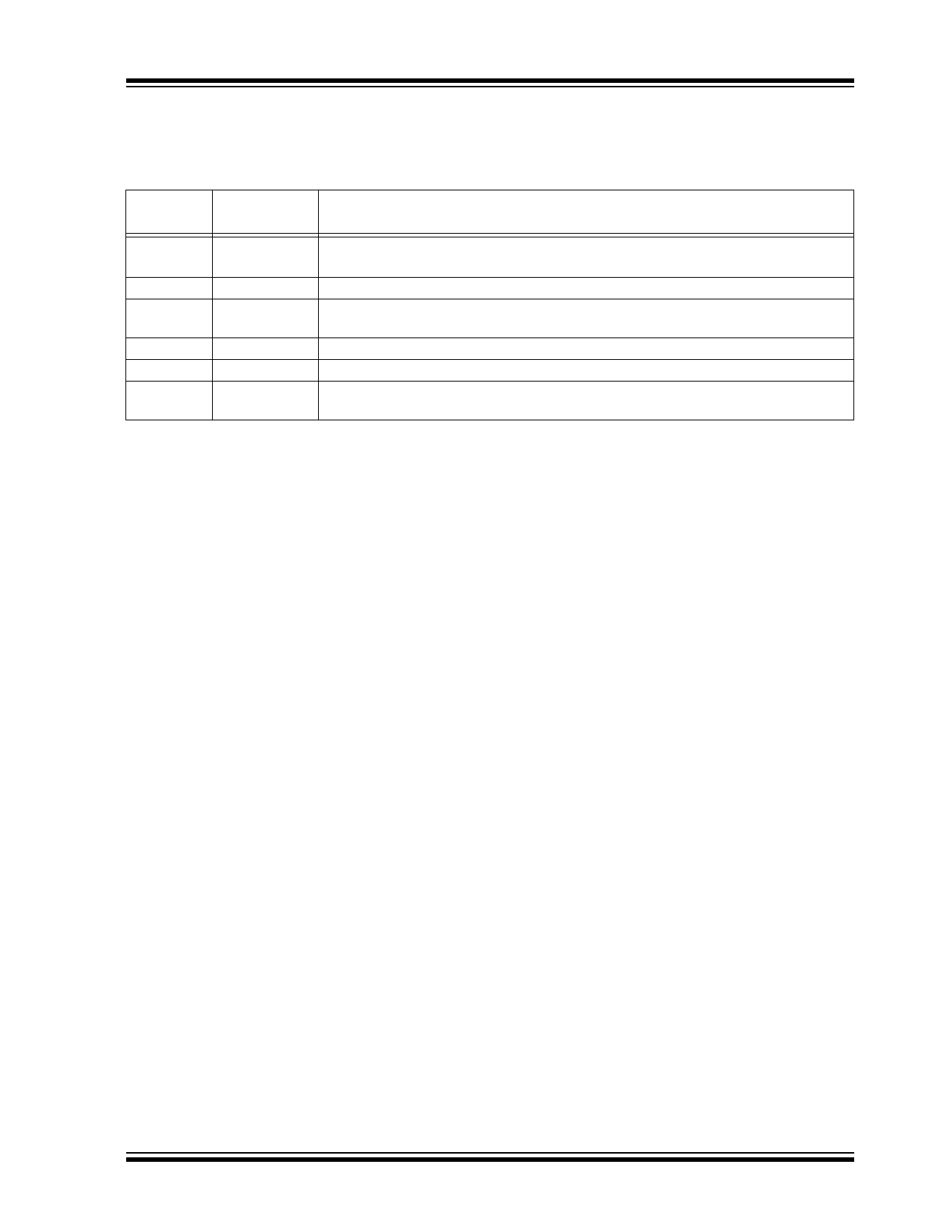
TABLE 3-1:
MCP16301
SOT-23
1
2
3
4
5
6
PIN FUNCTION TABLE
Symbol
Description
BOOST
GND
VFB
EN
VIN
SW
Boost voltage that drives the internal NMOS control switch. A bootstrap capacitor is
connected between the BOOST and SW pins.
Ground Pin
Output voltage feedback pin. Connect VFB to an external resistor divider to set the
output voltage.
Enable pin. Logic high enables the operation. Do not allow this pin to float.
Input supply voltage pin for power and internal biasing.
Output switch node, connects to the inductor, freewheeling diode and the bootstrap
capacitor.
3.1 Boost Pin (BOOST)
The high side of the floating supply used to turn the
integrated N-Channel MOSFET on and off is
connected to the boost pin.
3.2 Ground Pin (GND)
The ground or return pin is used for circuit ground
connection. The length of the trace from the input cap
return, output cap return and GND pin should be made
as short as possible to minimize the noise on the GND
pin.
3.3 Feedback Voltage Pin (VFB)
The VFB pin is used to provide output voltage regulation
by using a resistor divider. The VFB voltage will be
0.800V typical with the output voltage in regulation.
3.4 Enable Pin (EN)
The EN pin is a logic-level input used to enable or
disable the device switching, and lower the quiescent
current while disabled. A logic high (> 1.4V) will enable
the regulator output. A logic low (<0.4V) will ensure that
the regulator is disabled.
3.5 Power Supply Input Voltage Pin
(VIN)
Connect the input voltage source to VIN. The input
source should be decoupled to GND with a
4.7 µF - 20 µF capacitor, depending on the impedance
of the source and output current. The input capacitor
provides AC current for the power switch and a stable
voltage source for the internal device power. This
capacitor should be connected as close as possible to
the VIN and GND pins. For lighter load applications, a
1 µF X7R or X5R ceramic capacitor can be used.
3.6 Switch Pin (SW)
The switch node pin is connected internally to the
N-channel switch, and externally to the SW node
consisting of the inductor and Schottky diode. The SW
node can rise very fast as a result of the internal switch
turning on. The external Schottky diode should be
connected close to the SW node and GND.
© 2011 Microchip Technology Inc.
DS25004A-page 9
Share Link: 