NJM2871 データシートの表示(PDF) - Japan Radio Corporation
部品番号
コンポーネント説明
メーカー
NJM2871 Datasheet PDF : 8 Pages
| |||
NJM2871/A, NJM2872/A
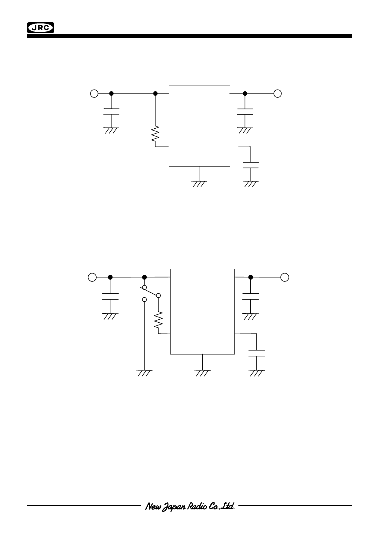
s TYPICAL APPLICATION
x In case that ON/OFF Control is not required:
VIN
VIN
VOUT
0.1uF
R
(0∼300kΩ)
CONTROL
NOISE
BYPASS
GND
VOUT
1.0uF *note1
(ceramic)
Cp=0.01uF
*note1 2.0V < Vo ≤ 2.6V version : Co=2.2uF(ceramic)
Vo ≤ 2.0V version : Co=4.7uF(ceramic)
Connect control terminal to VIN terminal
The quiescent current can be reduced by using a resistance “R”. Instead, it increases the minimum
operating voltage. For further information, please refer to Figure “Output Voltage vs. Control Voltage”.
y In use of ON/OFF CONTROL:
VIN
VIN
VOUT
VOUT
0.1uF
R
CONTROL
NOISE
BYPASS
GND
1.0uF *note1
(ceramic)
Cp=0.01uF
*note1 2.0V < Vo ≤ 2.6V version : Co=2.2uF(ceramic)
Vo ≤ 2.0V version : Co=4.7uF(ceramic)
State of control terminal:
•“H”→ output is enabled.
• “L” or “open” → output is disabled.
✱Noise bypass Capacitance Cp
Noise bypass capacitance Cp reduces noise generated by band-gap reference circuit.
Noise level and ripple rejection will be improved when larger Cp is used.
Use of smaller Cp value may cause oscillation.
Use the Cp value of 0.01uF greater to avoid the problem.
Share Link: 