HI1178 データシートの表示(PDF) - Intersil
部品番号
コンポーネント説明
メーカー
HI1178 Datasheet PDF : 11 Pages
| |||
HI1178
Absolute Maximum Ratings TA = 25oC
Supply Voltage (VDD) . . . . . . . . . . . . . . . . . . . . . . . . . . . . . . . . . .7V
Input Voltage (VIN). . . . . . . . . . . . . . . . . . . . . . . . . . . . . VDD to VSS
Output Current (IOUT) . . . . . . . . . . . . . . . . . . . . . . . . . . VDD to VSS
Digital Input Voltage (CLK) . . . . . . . . . . . . . . . . . . . . . 0mA to 15mA
(Every Each Channel)
Operating Conditions
Temperature Range (TOPR) . . . . . . . . . . . . . . . . . . . -40oC to 85oC
Supply Voltage
AVDD, AVSS . . . . . . . . . . . . . . . . . . . . . . . . . . . . . 4.75V to 5.25V
DVDD, DVSS . . . . . . . . . . . . . . . . . . . . . . . . . . . . 4.75V to 5.25V
Reference Input Voltage (VREF) . . . . . . . . . . . . . . . . . . . . . . . . . .2V
Clock Pulse Width
tPW1 . . . . . . . . . . . . . . . . . . . . . . . . . . . . . . . . . . . . . . 12.5ns (Min)
tPW0 . . . . . . . . . . . . . . . . . . . . . . . . . . . . . . . . . . . . . . 12.5ns (Min)
Thermal Information
Thermal Resistance (Typical, Note 1)
θJA (oC/W)
MQFP Package . . . . . . . . . . . . . . . . . . . . . . . . . . . .
94
Maximum Junction Temperature (Plastic Package) . . . . . . . .150oC
Maximum
Maximum
Storage Temperature Range (TSTG)
Lead Temperature (Soldering 10s) . .
.
.
.
.
.
.
-65oC
......
to
..
150oC
300oC
(MQFP - Lead Tips Only)
CAUTION: Stresses above those listed in “Absolute Maximum Ratings” may cause permanent damage to the device. This is a stress only rating and operation of the
device at these or any other conditions above those indicated in the operational sections of this specification is not implied.
NOTE:
1. θJA is measured with the component mounted on an evaluation PC board in free air.
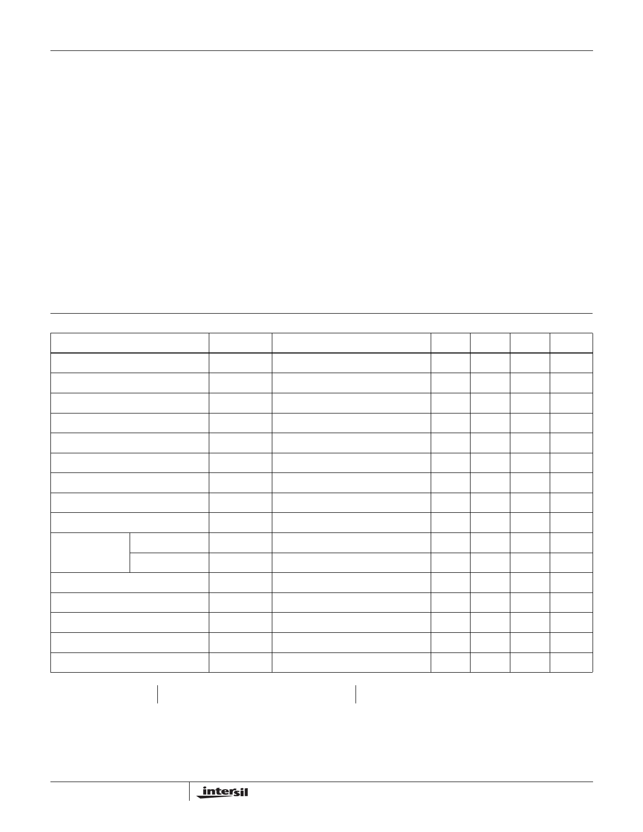
Electrical Specifications fCLK = 40MHz, VDD = 5V, ROUT = 200Ω, VREF = 2.0V, TA = 25oC
PARAMETER
SYMBOL
TEST CONDITIONS
MIN
TYP
MAX UNITS
Resolution
Maximum Conversion Speed
Linearity Error
Differential Linearity Error
Full Scale Output Voltage
Full Scale Output Ratio (Note 1)
Full Scale Output Current
Offset Output Voltage
Power Supply Current
Digital Input
Current
H Level
L Level
Set Up Time
Hold Time
Propagation Delay Time
Glitch Energy
Crosstalk
n
fMAX
EL
ED
VFS
FSR
IFS
VOS
IDD
IIH
IIL
tS
tH
tPD
GE
CT
14.3MHz, at Color Bar Data Input
ROUT = 75Ω
1MHz Sine Wave Output
-
8
-
bit
40
-
-
MSPS
-2.5
-
2.5
LSB
-0.3
-
0.3
LSB
1.8
2.0
2.2
V
0
1.5
3
%
-
10
15
mA
-
-
1
mV
-
-
48
mA
-
-
5
µA
-5
-
-
µA
5
-
-
ns
10
-
-
ns
-
10
-
ns
-
30
-
pV/s
-
57
-
dB
NOTE:
1. Full scale output ratio = ---------------------------F----u---l--l---S----c---a---l-e-----V----o----l-t--a---g---e-----o----f---C----h----a---n---n----e---l---------------------------–1 x 100(%)
Average of the Full Scale Voltage of the Channels
5
Share Link: 