AD7441 データシートの表示(PDF) - Analog Devices
部品番号
コンポーネント説明
メーカー
AD7441 Datasheet PDF : 24 Pages
| |||
AD7441/AD7451
TIMING SPECIFICATIONS1
VDD = 2.7 V to 5.25 V; fSCLK = 18 MHz; fS = 1 MSPS; VREF = 2.5 V; TA = TMIN to TMAX, unless otherwise noted.
Table 3.
Parameter
fSCLK 2
tCONVERT
tQUIET
t1
t2
t3 3
t4
t5
t6
t7
t8 4
tPOWER-UP 5
Limit at TMIN, TMAX
10
18
16 × tSCLK
888
60
10
10
20
40
0.4 tSCLK
0.4 tSCLK
10
10
35
1
Unit
kHz min
MHz max
ns max
ns min
ns min
ns min
ns max
ns max
ns min
ns min
ns min
ns min
ns max
μs max
Description
tSCLK = 1/fSCLK
Minimum quiet time between end of a serial read and next falling edge of CS
Minimum CS pulse width
CS falling edge to SCLK falling edge setup time
Delay from CS falling edge until SDATA three-state disabled
Data access time after SCLK falling edge
SCLK high pulse width
SCLK low pulse width
SCLK edge to data valid hold time
SCLK falling edge to SDATA, three-state enabled
SCLK falling edge to SDATA, three-state enabled
Power-up time from full power-down
1 Guaranteed by characterization. All input signals are specified with tRISE = tFALL = 5 ns (10% to 90% of VDD) and timed from a voltage level of 1.6 V. See Figure 2, Figure 3,
and the Serial Interface section.
2 Mark/space ratio for the SCLK input is 40/60 to 60/40.
3 Measured with the load circuit of Figure 4 and defined as the time required for the output to cross 0.8 V or 2.4 V with VDD = 5 V and the time required for an output to
cross 0.4 V or 2.0 V for VDD = 3 V.
4 t8 is derived from the measured time taken by the data outputs to change 0.5 V when loaded with the circuit of Figure 4. The measured number is then extrapolated
back to remove the effects of charging or discharging the 25 pF capacitor. This means that the time (t8) quoted in the timing characteristics is the true bus relinquish
time of the part and is independent of the bus loading.
5 See the Power-Up Time section.
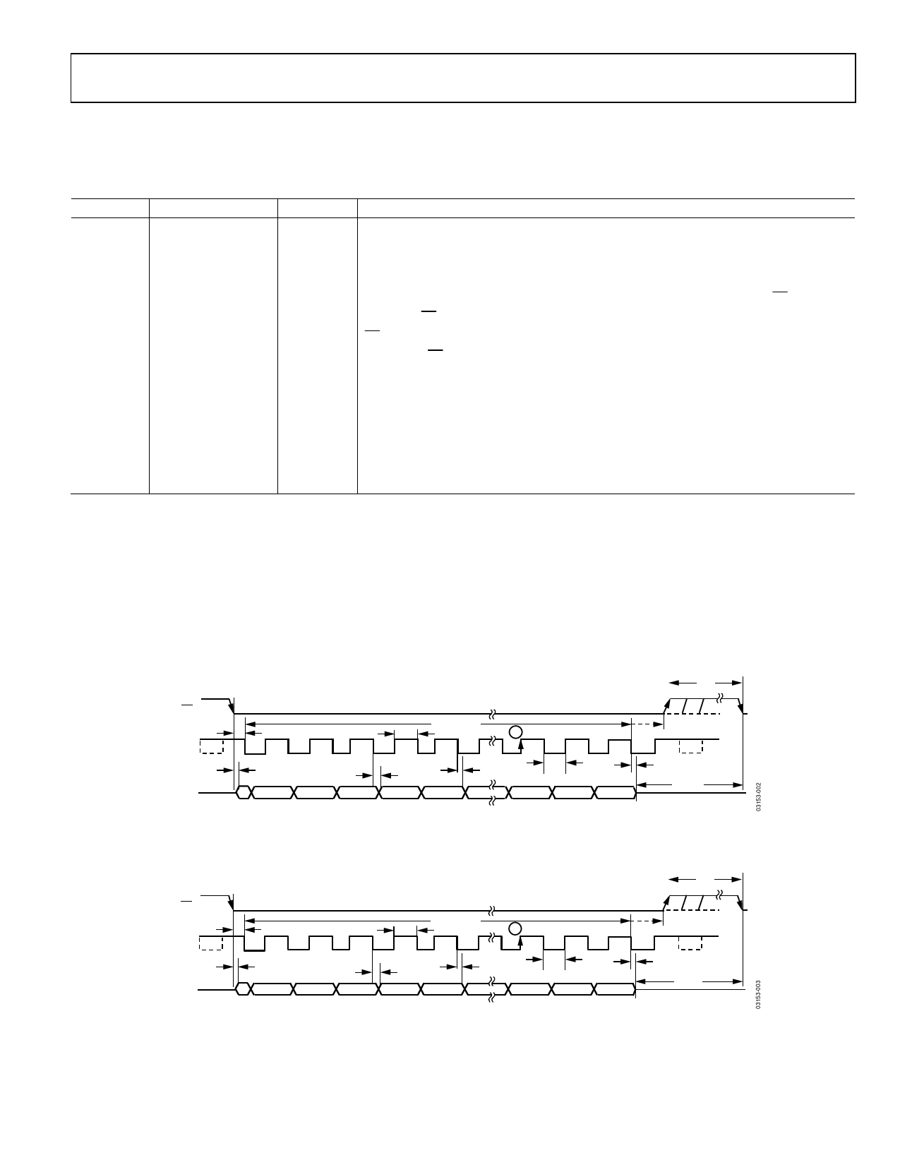
TIMING DIAGRAMS
CS
t2
SCLK
t3
SDATA
t1
tCONVERT
t5
B
1
2
3
4
5
13
14
t4
t7
t6
0
0
0
0
4 LEADING ZEROS
DB11
DB10
DB2
DB1
Figure 2. AD7451 Serial Interface Timing Diagram
15
t8
DB0
16
tQUIET
THREE-STATE
CS
t2
SCLK
t3
SDATA
t1
1
2
3
t4
0
0
0
0
4 LEADING ZEROS
t5
4
tCONVERT
5
t7
DB9
DB8
B
13
DB0
14
15
16
t6
t8
0
0
tQUIET
2 TRAILING ZEROS THREE-STATE
Figure 3. AD7441 Serial Interface Timing Diagram
Rev. D | Page 7 of 24
Share Link: 