EVAL-AD7453CB データシートの表示(PDF) - Analog Devices
部品番号
コンポーネント説明
メーカー
EVAL-AD7453CB Datasheet PDF : 20 Pages
| |||
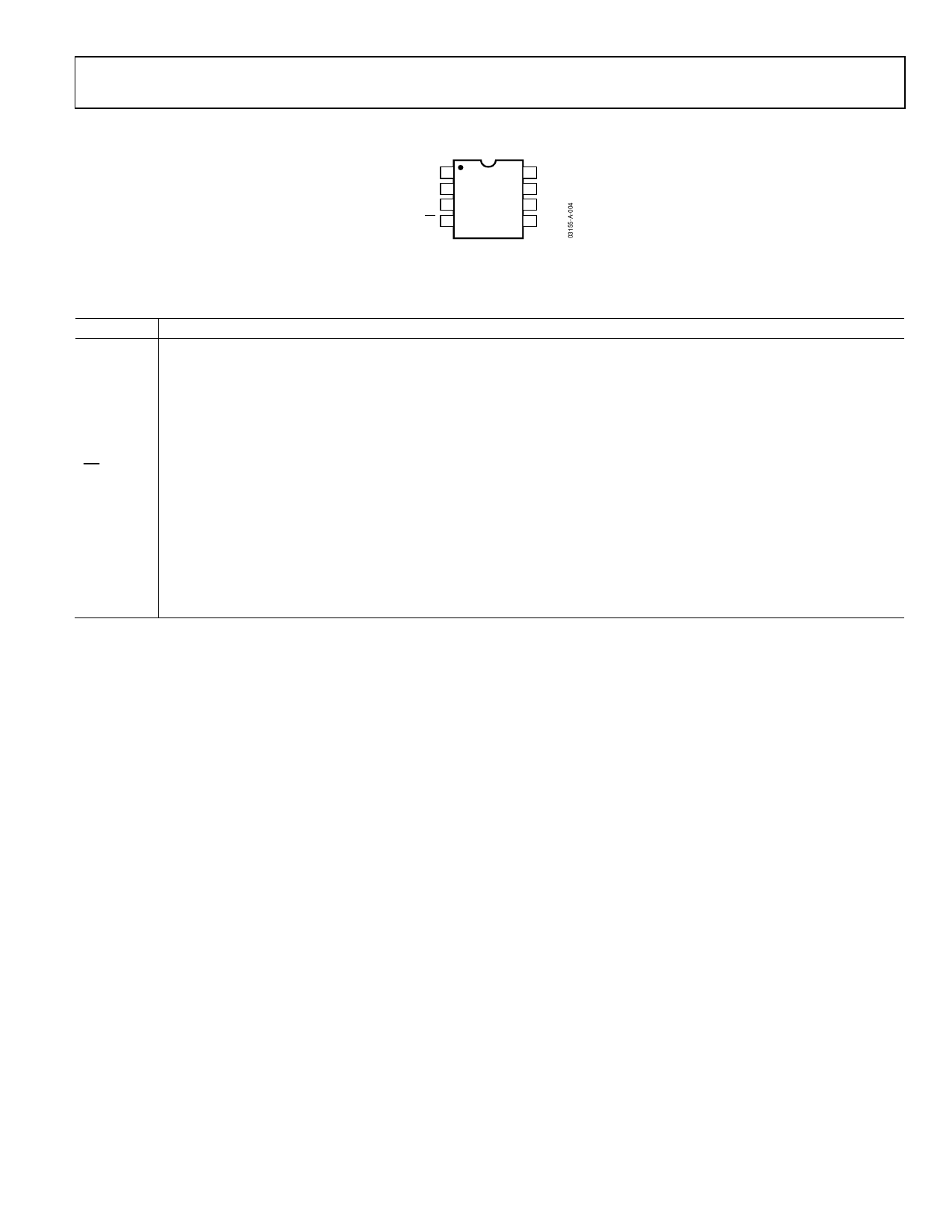
PIN CONFIGURATION AND FUNCTION DESCRIPTIONS
VDD 1
8 VREF
SCLK 2 AD7453 7 VIN+
SDATA 3 TOP VIEW 6 VIN–
(Not to Scale)
CS 4
5 GND
Figure 4. Pin Function Descriptions
AD7453
Table 4. Pin Function Descriptions
Mnemonic Function
VREF
Reference Input for the AD7453. An external reference in the range 100 mV to VDD must be applied to this input. The specified
reference input is 2.5 V. This pin should be decoupled to GND with a capacitor of at least 0.1 µF.
VIN+
Noninverting Analog Input.
VIN–
Inverting Input. This pin sets the ground reference point for the VIN+ input. Connect to ground or to a dc offset to provide a
pseudo ground.
GND
Analog Ground. Ground reference point for all circuitry on the AD7453. All analog input signals and any external reference
signal should be referred to this GND voltage.
CS
Chip Select. Active low logic input. This input provides the dual function of initiating a conversion on the AD7453 and
framing the serial data transfer.
SDATA
Serial Data. Logic output. The conversion result from the AD7453 is provided on this output as a serial data stream. The bits
are clocked out on the falling edge of the SCLK input. The data stream of the AD7453 consists of four leading zeros followed
by the 12 bits of conversion data that are provided MSB first. The output coding is straight (natural) binary.
SCLK
Serial Clock. Logic input. SCLK provides the serial clock for accessing data from the part. This clock input is also used as the
clock source for the conversion process.
VDD
Power Supply Input. VDD is 2.7 V to 5.25 V. This supply should be decoupled to GND with a 0.1 µF capacitor and a 10 µF
tantalum capacitor.
Rev. B | Page 7 of 20
Share Link: 