AD6643 データシートの表示(PDF) - Analog Devices
部品番号
コンポーネント説明
メーカー
AD6643 Datasheet PDF : 40 Pages
| |||
Data Sheet
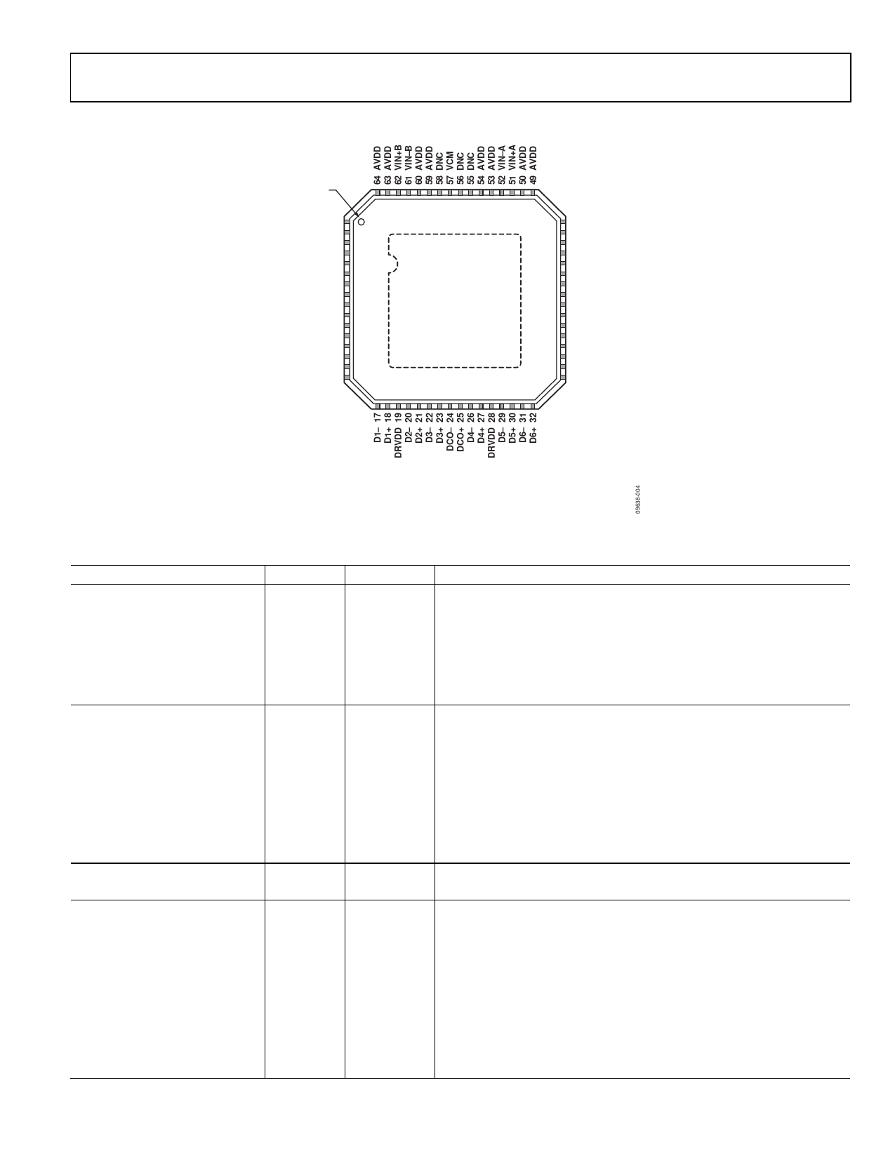
PIN CONFIGURATIONS AND FUNCTION DESCRIPTIONS
PIN 1
INDICATOR
CLK+ 1
CLK– 2
SYNC 3
DNC 4
DNC 5
DNC 6
DNC 7
DNC 8
DNC 9
DRVDD 10
DNC 11
DNC 12
DNC 13
DNC 14
D0– (LSB) 15
D0+ (LSB) 16
AD6643
INTERLEAVED
PARALLEL
LVDS
TOP VIEW
(Not to Scale)
48 PDWN
47 OEB
46 CSB
45 SCLK
44 SDIO
43 OR+
42 OR–
41 D10+ (MSB)
40 D10– (MSB)
39 D9+
38 D9–
37 DRVDD
36 D8+
35 D8–
34 D7+
33 D7–
AD6643
NOTES
1. DNC = DO NOT CONNECT. DO NOT CONNECT TO THIS PIN.
2. THE EXPOSED THERMAL PADDLE ON THE BOTTOM OF THE PACKAGE
PROVIDES THE ANALOG GROUND FOR THE PART. THIS EXPOSED PADDLE
MUST BE CONNECTED TO GROUND FOR PROPER OPERATION.
Figure 4. Pin Configuration (Top View), LFCSP Interleaved Parallel LVDS
Table 8. Pin Function Descriptions for the Interleaved Parallel LVDS Mode
Pin No.
Mnemonic Type
Description
ADC Power Supplies
10, 19, 28, 37
DRVDD
Supply
Digital Output Driver Supply (1.8 V Nominal).
49, 50, 53, 54, 59, 60, 63, 64 AVDD
Supply
Analog Power Supply (1.8 V Nominal).
4 to 9, 11 to 14, 55, 56, 58
DNC
Do Not Connect. Do not connect to these pins.
0
AGND,
Ground
Analog Ground. The exposed thermal paddle on the bottom of the
Exposed
package provides the analog ground for the device. This exposed paddle
Paddle
must be connected to ground for proper operation.
ADC Analog
51
VIN+A
Input
Differential Analog Input Pin (+) for Channel A.
52
VIN−A
Input
Differential Analog Input Pin (−) for Channel A.
62
VIN+B
Input
Differential Analog Input Pin (+) for Channel B.
61
VIN−B
Input
Differential Analog Input Pin (−) for Channel B.
57
VCM
Output
Common-Mode Level Bias Output for Analog Inputs. This pin should be
decoupled to ground using a 0.1 μF capacitor.
1
CLK+
Input
ADC Clock Input—True.
2
CLK−
Input
ADC Clock Input—Complement.
Digital Input
3
SYNC
Input
Digital Synchronization Pin. Slave mode only.
Digital Outputs
15
D0− (LSB) Output
Channel A/Channel B LVDS Output Data 0—True.
16
D0+ (LSB) Output
Channel A/Channel B LVDS Output Data 0—Complement.
18
D1+
Output
Channel A/Channel B LVDS Output Data 1—True.
17
D1−
Output
Channel A/Channel B LVDS Output Data 1—Complement.
21
D2+
Output
Channel A/Channel B LVDS Output Data 2—True.
20
D2−
Output
Channel A/Channel B LVDS Output Data 2—Complement.
23
D3+
Output
Channel A/Channel B LVDS Output Data 3—True.
22
D3−
Output
Channel A/Channel B LVDS Output Data 3—Complement.
27
D4+
Output
Channel A/Channel B LVDS Output Data 4—True.
Rev. C | Page 11 of 40
Share Link: 