AD7476 データシートの表示(PDF) - Analog Devices
部品番号
コンポーネント説明
メーカー
AD7476 Datasheet PDF : 20 Pages
| |||
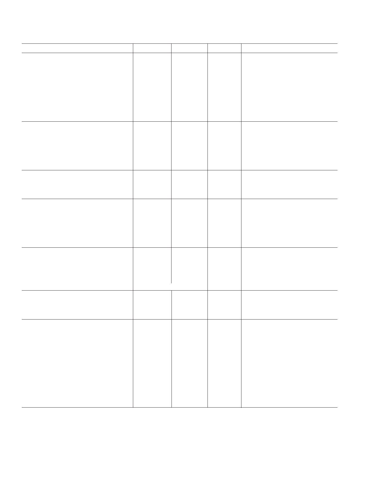
AD74786–SPECIFICATIONS1 (VDD = 2.7 V to 5.25 V, fSCLK= 20 MHz, TA = TMIN to TMAX, unless otherwise noted.)
Parameter
A Version1, 2 S Version1, 2
DYNAMIC PERFORMANCE
Signal-to-(Noise + Distortion) (SINAD)
49
49
Total Harmonic Distortion (THD)
–65
–65
Peak Harmonic or Spurious Noise (SFDR)
–65
–65
Intermodulation Distortion (IMD)
Second-Order Terms
–68
–68
Third-Order Terms
–68
–68
Aperture Delay
10
10
Aperture Jitter
30
30
Full Power Bandwidth
6.5
6.5
DC ACCURACY
Resolution
Integral Nonlinearity
Differential Nonlinearity
Offset Error
Gain Error
Total Unadjusted Error (TUE)
8
8
± 0.5
± 0.5
± 0.5
± 0.5
± 0.5
± 0.5
± 0.5
± 0.5
± 0.5
± 0.5
ANALOG INPUT
Input Voltage Ranges
DC Leakage Current
Input Capacitance
0 to VDD
±1
30
0 to VDD
±1
30
LOGIC INPUTS
Input High Voltage, VINH
Input Low Voltage, VINL
Input Current, IIN, SCLK Pin
Input Current, IIN, CS Pin
Input Capacitance, CIN4
LOGIC OUTPUTS
Output High Voltage, VOH
Output Low Voltage, VOL
Floating-State Leakage Current
Floating-State Output Capacitance4
Output Coding
2.4
2.4
0.8
0.8
0.4
0.4
±1
±1
±1
±1
10
10
VDD – 0.2
0.4
VDD – 0.2
0.4
± 10
± 10
10
10
Straight (Natural) Binary
CONVERSION RATE
Conversion Time
Track-and-Hold Acquisition Time
Throughput Rate
800
800
400
400
1
1
POWER REQUIREMENTS
VDD
IDD
Normal Mode (Static)
Normal Mode (Operational)
Full Power-Down Mode
Power Dissipation5
Normal Mode (Operational)
Full Power-Down
2.7/5.25
2
1
3.5
1.6
1
80
17.5
4.8
5
2.7/5.25
2
1
3.5
1.6
1
80
17.5
4.8
5
NOTES
1Temperature ranges as follows: A Version: –40°C to +85°C; S Version: –55°C to +125°C.
2Operational from VDD = 2.0 V, with input high voltage, VINH = 1.8 V min.
3See Terminology section.
4Guaranteed by characterization.
5See Power vs. Throughput Rate section.
Specifications subject to change without notice.
Unit
dB min
dB max
dB max
dB typ
dB typ
ns typ
ps typ
MHz typ
Test Conditions/Comments
fIN = 100 kHz Sine Wave, fSAMPLE = 1 MSPS
fa = 498.7 kHz, fb = 508.7 kHz
fa = 498.7 kHz, fb = 508.7 kHz
@ 3 dB
Bits
LSB max
LSB max
LSB max
LSB max
LSB max
Guaranteed No Missed Codes to Eight Bits
V
µA max
pF typ
V min
V max
V max
µA max
µA typ
pF max
VDD = 5 V
VDD = 3 V
Typically 10 nA, VIN = 0 V or VDD
V min
V max
µA max
pF max
ISOURCE = 200 µA; VDD = 2.7 V to 5.25 V
ISINK = 200 µA
ns max
16 SCLK Cycles with SCLK at 20 MHz
ns max
MSPS max See Serial Interface Section
V min/max
mA typ
mA typ
mA max
mA max
µA max
µA max
Digital I/Ps = 0 V or VDD
VDD = 4.75 V to 5.25 V; SCLK On or Off
VDD = 2.7 V to 3.6 V; SCLK On or Off
VDD = 4.75 V to 5.25 V; fSAMPLE = 1 MSPS
VDD = 2.7 V to 3.6 V; fSAMPLE = 1 MSPS
SCLK Off
SCLK On
mW max
mW max
µW max
VDD = 5 V; fSAMPLE = 1 MSPS
VDD = 3 V; fSAMPLE = 1 MSPS
VDD = 5 V; SCLK Off
–4–
REV. D
Share Link: 