2SK2085 データシートの表示(PDF) - Renesas Electronics
部品番号
コンポーネント説明
メーカー
2SK2085 Datasheet PDF : 12 Pages
| |||
2SK2085
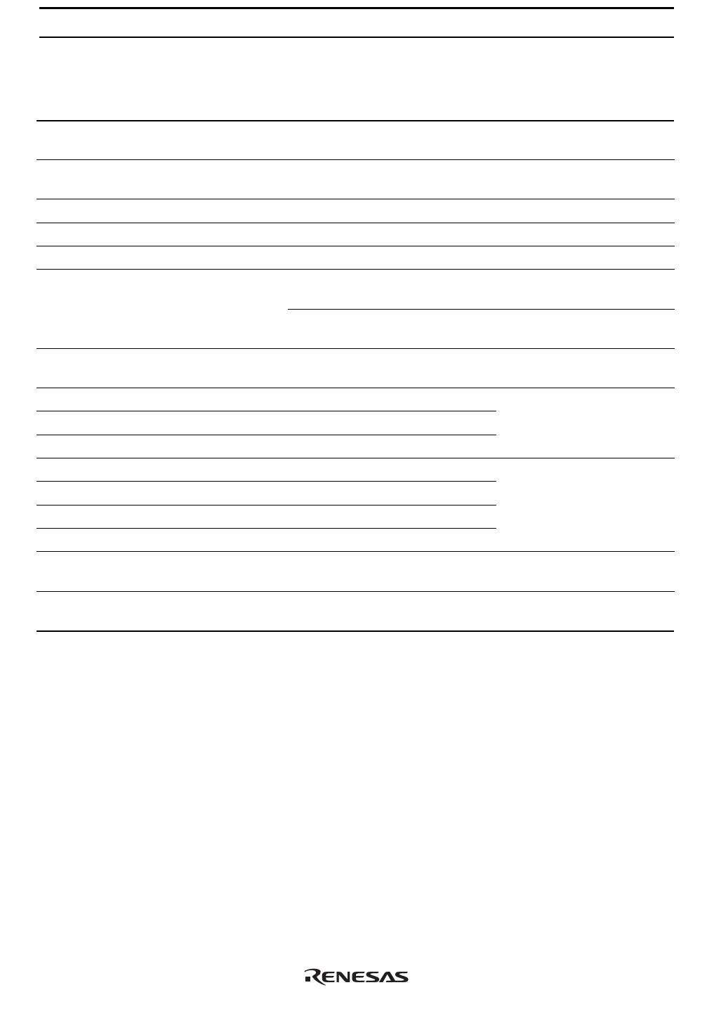
Electrical Characteristics (Ta = 25°C)
Item
Symbol Min
Drain to source breakdown
voltage
V(BR)DSS
100
Gate to source breakdown
voltage
V(BR)GSS
±20
Gate to source leak current IGSS
—
Zero gate voltage drain current IDSS
—
Gate to source cutoff voltage VGS(off)
1.0
Static drain to source on state RDS(on)
—
resistance
—
Typ
—
—
—
—
—
0.6
0.75
Forward transfer admittance |yfs|
0.7 1.2
Input capacitance
Ciss
—
Output capacitance
Coss —
Reverse transfer capacitance Crss
—
Turn-on delay time
t d(on)
—
Rise time
tr
—
Turn-off delay time
t d(off)
—
Fall time
tf
—
Body to drain diode forward VDF
—
voltage
Body to drain diode reverse trr
—
recovery time
Note 1. Pulse Test
130
50
12
7
6.5
55
20
0.85
80
Max
—
—
±10
100
2.0
0.9
1.35
—
—
—
—
—
—
—
—
—
—
Unit
V
V
µA
µA
V
S
pF
pF
pF
ns
ns
ns
ns
V
ns
Test conditions
ID = 10 mA, VGS = 0
IG = ±100 µA, VDS = 0
VGS = ±16 V, VDS = 0
VDS = 80 V, VGS = 0
ID = 1 mA, VDS = 10 V
ID = 0.5 A
VGS = 10 V*1
ID = 0.5 A
VGS = 4 V*1
ID = 0.5 A
VDS = 10 V*1
VDS = 10 V
VGS = 0
f = 1 MHz
ID = 0.5 A
VGS = 10 V
RL = 60
IF = 1.0 A, VGS = 0
IF = 1.0 A, VGS = 0,
diF / dt = 50 A / µs
Share Link: 