SC14480 データシートの表示(PDF) - Unspecified
部品番号
コンポーネント説明
メーカー
SC14480 Datasheet PDF : 259 Pages
| |||
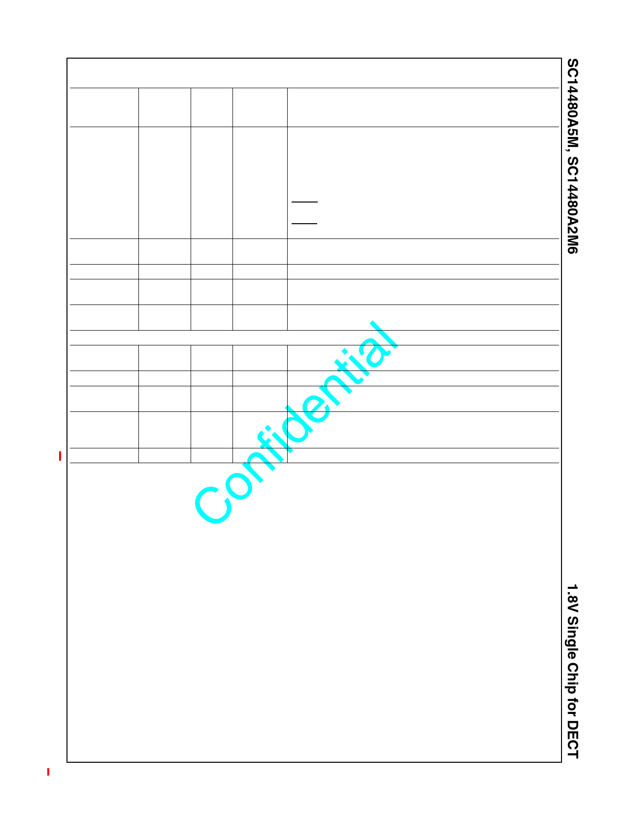
Table 1: Pin Description
PIN NAME
TYPE
Drive
(mA)
Reset
state
(Note 2)
DESCRIPTION
RF_SUPPLY
A7
INPUT Battery supply 1.9V-3.45V. Connected to VBAT if
<3.45V. Connected to collector of optional NPN transistor in case
3.45V<VBAT<5.5V. Pin 12 and Pin 71 must be connected
together (preferably directly to the 2-cell battery).
Only use LDO-RF for Li-ion headset applications when the load
current is small (no RF-PA and no class-D connected to it)
Pin 71 supplies LDOs for image reject mixer, RF port 2, 3, 4, 0n,
LNA, VCO, Phase frequency detector, PA driver.
Pin 12 supplies LDOs for IF filter, RX ADC, RF ports 0 and 1, fre-
quency divider, MMC, LDO Xtal.
AVD
A1
Codec Analog Frontend End and ADC Supply voltage. Internally
startpoint connected to VDD
VDD
A1
Digital Core and Digital PAD supply (VDDIO) voltage
VSS
A1
-
-
Digital ground and LDO_XTAL ground, all connected to GND
plane
GND Plane
-
-
-
Common ground for all circuits, except VSS_LNA, AVS_XTAL,
Xtal
l AVD_XTAL
A6
tia AVS_XTAL
A6
-
XTAL1
n XTAL2
A6
-
BXTAL
DO-BP
8
fide N.C>
VREFm, VSS_PADR.
-
-
I
I-PU
OUTPUT Supply voltage (1.7V) LDO for XTAL. Must be decou-
pled with 1uF ceramic capacitor.
Analog ground AVD_XTAL
INPUT 10.368/20.736 MHz crystal connection.
See chapter XTAL Oscillator.
OUTPUT. Digital buffered Xtal oscillator, can be switched on/off
using DIP <RF_EN>/<RF_DIS> instructions. This pin is not opti-
mized as reference clock for external RF devices
Not connected, VDD or VSS
Con Note 2:
All digital outputs can sink/source 2 mA unless otherwise specified. All digital inputs have Schmitt trigger inputs. After reset all I/Os are set
to input and all pull-up or pull-down resistors are enabled unless otherwise specified.
PU = Pull-up resistor enabled, PD = Pull-down resistor enabled, I = input,
O=output, Hi-Z= high impedance, 1= logic HIGH level, 0= logic LOW level
Refer also to Px_DIR_REGs for INPUT/OUTPUT and Pull-up/Pull-down configurations
Note 3: Backdrive protected pins allow always interfacing with devices using VDDIO upto 3.45V.
If PAD_CTRL_REG[xxx_OD] bit is set then 1) the internal Pull-up resistors are always disabled to prevent currents from 1.8V< Vin <3.45 to
VDD.
2) If port is set to output, the output is always configured as opendrain to allow the output level to reach VDDIO >1.8V. The external pull-up
resistor value determines the rise time of the signal.
Note 4: For basestation applications with high line input voltages, an input protecton on all ADC inputs can be enabled with
AD_CTRL_REG[ADCx_PR_DIS] =’0’. To limit the input current as specified in chapter “specifications”, an external resistor must placed in
series with the ADC inputs. With the input protection enabled, the ADC is linear from 0 to 0.9V. With ADCx_PR_DIS=’1’ the ADC0 and
ADC1 are linear from 0-1.8V, but ADC2 is linear from 0-1.35V due to a voltage limiter which protects the ADC input for the NTC input above
1.8V.
Note 5: In digital mode extra static VDDPA current will flow (See Supply currents (Indicative value) (table 275, page 221)). So the digital mode is not
recommended in portable applications.
Note 6: The reason for this output overvoltage protection is that a speaker is an inductor (which can store energy). In case the battery is removed
from the handset while handsfree speaker is active, the battery voltage could become too high when the inductor releases its energy to the
battery (which is not present anymore as a buffer). To prevent this electrical overstress situation, the overvoltage protection is added
© 2008-2009 SiTel Semiconductor
11
Version: January 21, 2009 v1.0
Share Link: 