SC14480 データシートの表示(PDF) - Unspecified
部品番号
コンポーネント説明
メーカー
SC14480 Datasheet PDF : 259 Pages
| |||
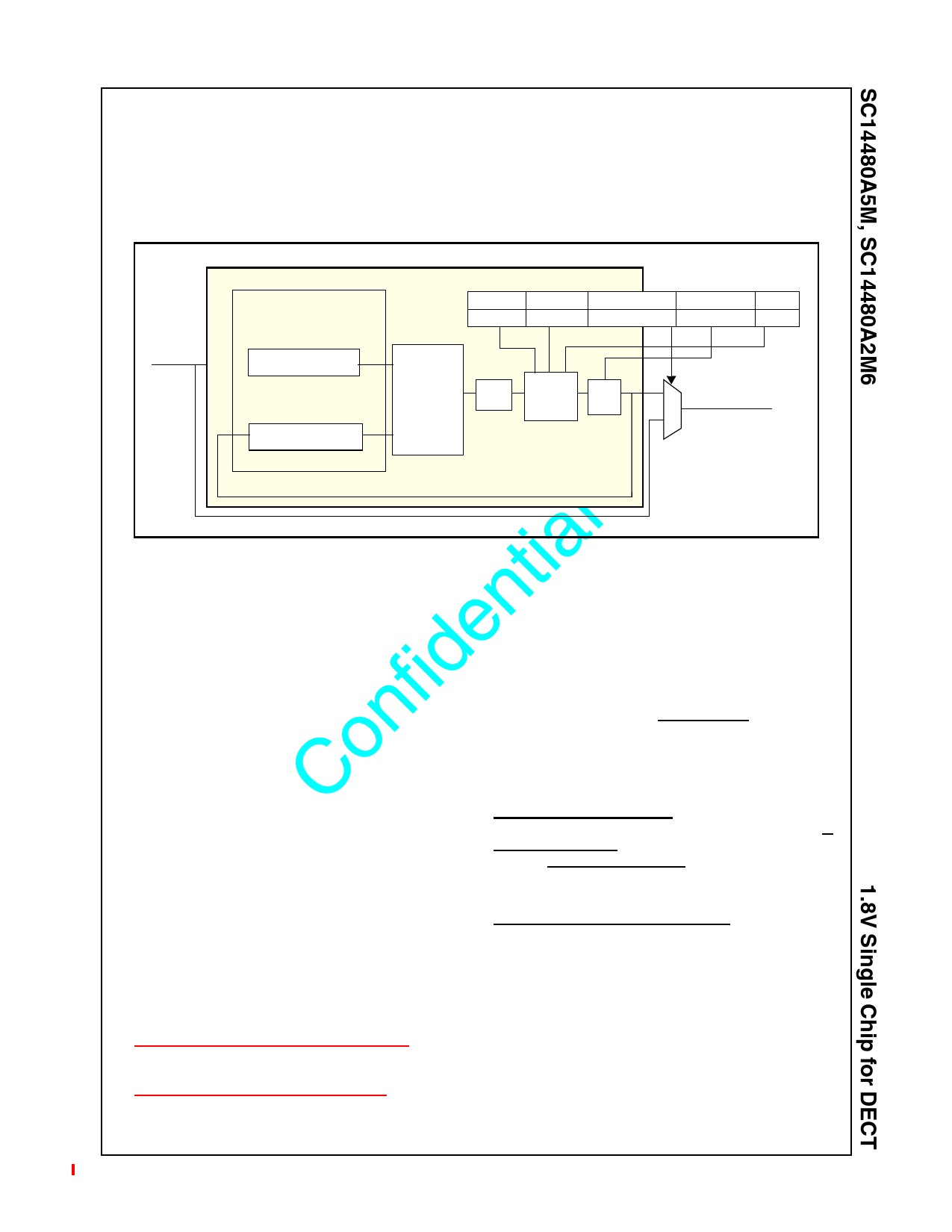
3.6 PHASE LOCKED LOOP (PLL)
The SC14480A5M, SC14480A2M6 contains a Phase
Locked Loops (PLL) that is depicted in Figure 6: The
PLL generates a clock with a frequency x16, x8 or x4
higher than the Xtal frequency, i.e., 165,888 or 82.944
or or 82.944/2 MHz.
The PLL is not required during a normal voice connec-
tion for a basic DECT cordless telephone. However, the
PLL can be used if a higher cycle budget on the
CR16Cplus or Gen2DSP is required, e.g., for hands-
free applications.
.
Fxtal
PLL_DIV_REG
1
0
XD
5
2
VD
CLK_PLL_CTRL_REG
6
4
3
2
1
HF_SEL VCO_ON PLL_CLK_SEL PLL_OUT_DIV CP_ON
phase
com-
parator.
lpf
Fupd
VCO
/1, /2
Fpll
1 Fsys
0
clock switch
tial Figure 6 PLL block diagram
3.7 PLL CLOCK SWITCHING
n At startup the PLL is bypassed (PLL_CLK_SEL=0) and
the xtal frequency clocks the whole IC. The dividers
e CLK_CODEC_DIV_REG[CODEC_CLK_DIV],
fid PER_DIV_REG[PER_DIV] must be set according
Table 6 on page 21 to get the fundamental 1.152 MHz
for Codec and peripherals.
n If the PLL is switched as system clock Fsys with
PLL_CLK_SEL=1, the output frequency of CLKN_DIV
o is kept constant to the 10.368 MHz DIP frequency
FDIP, the 1.152 MHz for peripherals and 10.368 MHz
C for the UART 230kbaud and SPI.
PLL_OUT_DIV for 41.472 MHz output.
• VCO and charge pump can be switched on with
CLK_PLL_CTRL_REG[4] = VCO_ON set to 1 and
CLK_PLL_CTRL_REG[1] = CP_ON set to 1.
CLK_PLL_CTRL_REG[2] = PLL_DIV_OUT must be
set to 1 to get 41.472 MHz with VCO 82.944 Mhz
• The firmware must wait at least 500 us before
PLL_CLK_SEL may be set to 1. This time is needed
for the PLL to settle to the Fpll frequency.
• CLK_PLL_CTRL_REG[3] = PLL_CLK_SEL is 1 to
use the PLL clock as system clock
This seamless dynamic clock switching can be done
while a MAC link is active. Switching from xtal to the
PLL clock stretches the DECT bitclock with 1 PLL clock
cycle. Switching from PLL to xtal clock shortens the
DECT bitclock with 1 PLL bitclock.
Switching back to xtal mode can be done at any time
by setting PLL_CLK_SEL to 0. The CR16 must wait at
least 10 PLL cycles (E.g 5xNOP if CLK_DIV=1) if DIP
is off or 2 DIP Bit clock cycles (c.q 1.75 us in case of
DECT) if PLL is on before the VCO and Charge Pump
may be switched off.
3.8 PLL CLOCK SWITCHING PROCEDURE
The sequence to enable and disable the PLL is:
Change clock frequency during a link is only possible
via XTAL mode (PLLCLK_SEL=0), then the new PLL
• The PLL starts up in the bypass mode with
CLK_PLL_CTRL_REG[3] = PLL_CLK_SEL is 0
frequency must be set according to the clock switching
procedure described above.
• For 10.368 MHz XTAL frequency (and 20.736/2),
Set PLL Xtal divider XD and VCO divider VD:
CLK_PLL_DIV_REG = 0x1C for 165.888 MHz
CLK_PLL_DIV_REG = 0x8 for 124.416 MHz
CLK_PLL_DIV_REG = 0x4 (recommended) or 0x1D
for 82.944 MHz
CLK_PLL_DIV_REG = 5 for 41.472 MHz
CLK_PLL1_DIV_REG = 0x4 for 82.944 MHz and set
© 2008-2009 SiTel Semiconductor
20
Version: January 21, 2009 v1.0
Share Link: 