IRS21531DSPBF データシートの表示(PDF) - International Rectifier
部品番号
コンポーネント説明
メーカー
IRS21531DSPBF Datasheet PDF : 14 Pages
| |||
IRS2153(1)D
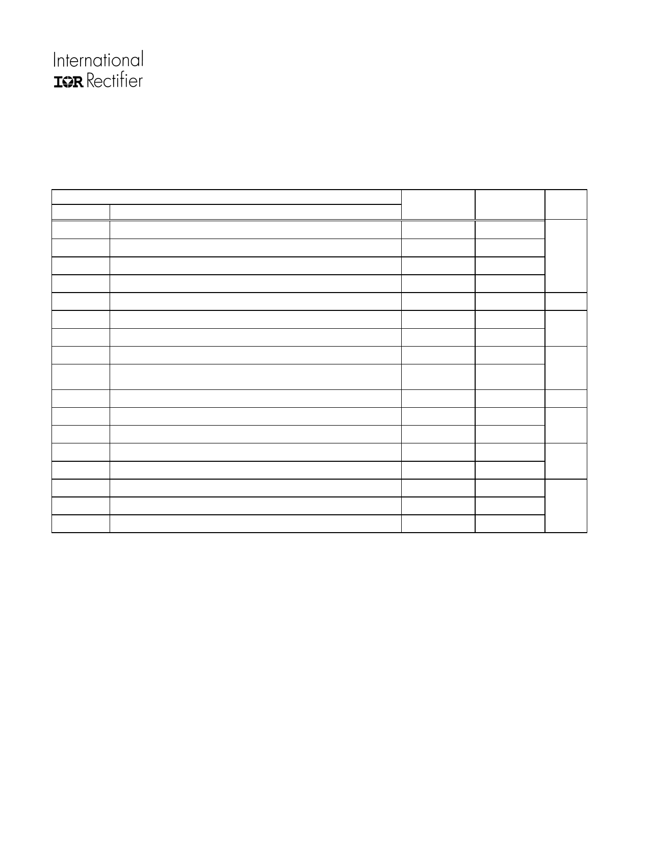
Absolute Maximum Ratings
Absolute maximum ratings indicate sustained limits beyond which damage to the device may occur. All
voltage parameters are absolute voltages referenced to COM, all currents are defined positive into any lead.
The thermal resistance and power dissipation ratings are measured under board mounted and still air
conditions.
Symbol
Parameter
Definition
Min.
Max. Units
VB High side floating supply voltage
VS High side floating supply offset voltage
VHO High side floating output voltage
VLO Low side output voltage
IRT RT pin current
-0.3
VB - 25
VS – 0.3
-0.3
-5
625
VB + 0.3
V
VB + 0.3
VCC + 0.3
5
mA
VRT
VCT
ICC
IOMAX
dVS/dt
PD
PD
RthJA
RthJA
TJ
TS
TL
RT pin voltage
CT pin voltage
Supply current (Note 1)
Maximum allowable current at LO and HO due to external
power transistor Miller effect.
Allowable offset voltage slew rate
Maximum power dissipation @ TA ≤ +25 ºC, 8-Pin DIP
Maximum power dissipation @ TA ≤ +25 ºC, 8-Pin SOIC
Thermal resistance, junction to ambient, 8-Pin DIP
Thermal resistance, junction to ambient, 8-Pin SOIC
Junction temperature
Storage temperature
Lead temperature (soldering, 10 seconds)
-0.3
-0.3
---
-500
-50
---
---
---
---
-55
-55
---
VCC + 0.3
VCC + 0.3
20
500
50
1.0
0.625
85
128
150
150
300
V
mA
V/ns
W
ºC/W
ºC
Note 1: This IC contains a zener clamp structure between the chip VCC and COM which has a nominal
breakdown voltage of 15.4 V. Please note that this supply pin should not be driven by a DC, low
impedance power source greater than the VCLAMP specified in the Electrical Characteristics section.
2
Share Link: 