11N60(2017) データシートの表示(PDF) - Alpha and Omega Semiconductor
部品番号
コンポーネント説明
メーカー
11N60 Datasheet PDF : 6 Pages
| |||
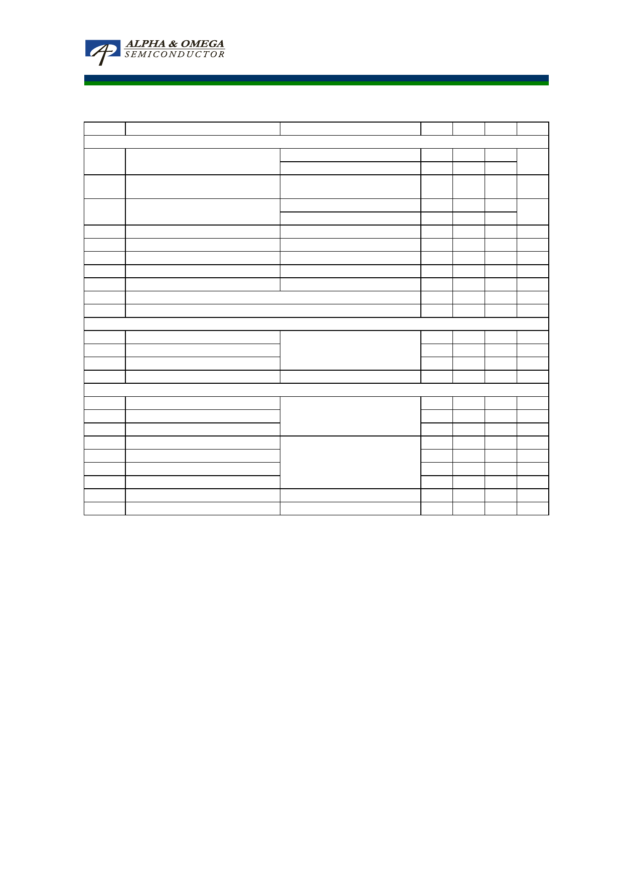
Electrical Characteristics (TJ=25°C unless otherwise noted)
Symbol
Parameter
Conditions
Min Typ Max Units
STATIC PARAMETERS
BVDSS Drain-Source Breakdown Voltage
ID=250µA, VGS=0V, TJ=25°C
ID=250µA, VGS=0V, TJ=150°C
BVDSS
/∆TJ
Breakdown Voltage Temperature
Coefficient
ID=250µA, VGS=0V
IDSS
Zero Gate Voltage Drain Current
VDS=600V, VGS=0V
VDS=480V, TJ=125°C
IGSS
VGS(th)
Gate-Body leakage current
Gate Threshold Voltage
VDS=0V, VGS=±30V
VDS=5V ID=250µA
RDS(ON)
gFS
VSD
Static Drain-Source On-Resistance
Forward Transconductance
Diode Forward Voltage
VGS=10V, ID=5.5A
VDS=40V, ID=5.5A
IS=1A,VGS=0V
IS
Maximum Body-Diode Continuous Current
ISM
Maximum Body-Diode Pulsed Current
DYNAMIC PARAMETERS
Ciss
Input Capacitance
Coss
Output Capacitance
VGS=0V, VDS=25V, f=1MHz
Crss
Reverse Transfer Capacitance
Rg
Gate resistance
VGS=0V, VDS=0V, f=1MHz
SWITCHING PARAMETERS
Qg
Total Gate Charge
Qgs
Gate Source Charge
VGS=10V, VDS=480V, ID=11A
Qgd
Gate Drain Charge
tD(on)
tr
tD(off)
Turn-On DelayTime
Turn-On Rise Time
Turn-Off DelayTime
VGS=10V, VDS=300V, ID=11A,
RG=25Ω
tf
Turn-Off Fall Time
trr
Body Diode Reverse Recovery Time IF=11A,dI/dt=100A/µs,VDS=100V
Qrr
Body Diode Reverse Recovery Charge IF=11A,dI/dt=100A/µs,VDS=100V
600
700
V
0.67
V/ oC
1
10
µA
±100 nΑ
3.3 3.9 4.5
V
0.56 0.65 Ω
12
S
0.73 1
V
11
A
39
A
1320 1656 1990 pF
100 146 195 pF
6.5 11.2 16 pF
1.7 3.5 5.3
Ω
24 30.6 37 nC
9.6
nC
9.6
nC
39
ns
58
ns
92
ns
42
ns
400 500 600 ns
4.7
5.9 7.1
µC
A. The value of R θJA is measured with the device in a still air environment with T A =25°C.
B. The power dissipation PD is based on TJ(MAX)=150°C, using junction-to-case thermal resistance, and is more useful in setting the upper
dissipation limit for cases where additional heatsinking is used.
C. Repetitive rating, pulse width limited by junction temperature TJ(MAX)=150°C, Ratings are based on low frequency and duty cycles to keep initial
TJ =25°C.
D. The R θJA is the sum of the thermal impedence from junction to case R θJC and case to ambient.
E. The static characteristics in Figures 1 to 6 are obtained using <300 µs pulses, duty cycle 0.5% max.
F. These curves are based on the junction-to-case thermal impedence which is measured with the device mounted to a large heatsink, assuming a
maximum junction temperature of TJ(MAX)=150°C. The SOA curve provides a single pulse rating.
G. L=60mH, IAS=4.8A, VDD=150V, RG=25Ω, Starting TJ=25°C
APPLICATIONS OR USE AS CRITICAL COMPONENTS IN LIFE SUPPORT DEVICES OR SYSTEMS ARE NOT AUTHORIZED. AOS DOES NOT
ASSUME ANY LIABILITY ARISING OUT OF SUCH APPLICATIONS OR USES OF ITS PRODUCTS. AOS RESERVES THE RIGHT TO IMPROVE
PRODUCT DESIGN,FUNCTIONS AND RELIABILITY WITHOUT NOTICE.
Rev 1.0: Sepetember 2017
www.aosmd.com
Page 2 of 6
Share Link: 