HD74BC645 データシートの表示(PDF) - Renesas Electronics
部品番号
コンポーネント説明
メーカー
HD74BC645 Datasheet PDF : 8 Pages
| |||
HD74BC645A
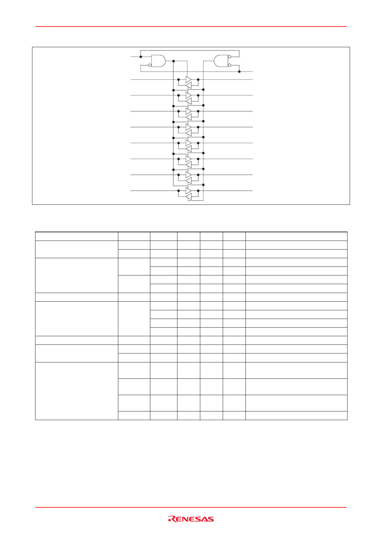
Logic Diagram
DiR
G
A1
B1
A2
B2
A3
B3
A4
B4
A5
B5
A6
B6
A7
B7
A8
B8
Electrical Characteristics (Ta = –40 to +85°C)
Item
Input voltage
Output voltage
Input diode voltage
Input current
Output short circuit current*1
Off state output current
Supply current
Symbol
VIH
VIL
VOH
VOL
VIK
II
IOS
IOZH
IOZL
ICCL
VCC (V)
4.5
4.5
4.5
4.5
4.5
5.5
5.5
5.5
5.5
5.5
5.5
5.5
5.5
Min
2.0
—
2.4
2.0
—
—
—
—
—
—
—
–100
—
—
—
Max
—
0.8
—
—
0.5
0.55
–1.2
–250
100
1.0
100
–225
–100
–250
31.5
Unit
V
V
V
V
V
V
V
µA
µA
µA
µA
mA
µA
µA
mA
Test Conditions
IOH = –3 mA
IOH = –15 mA
IOL = 48 mA
IOL = 64 mA
IIN = –18 mA
VIN = 0 V
An or Bn, VIN = 5.5 V
DiR or G, VIN = 5.5 V
DiR or G, VIN = 7 V
VO = 0 V, VIN = 0 or 5.5 V
VO = 2.7 V
VO = 0.5 V
VIN = 0 or 5.5 V
All outputs is “L”
ICCH
5.5
—
0.5
mA
VIN = 0 or 5.5 V
All outputs is “H”
ICCZ
5.5
—
4.5
mA
VIN = 0 or 5.5 V
All outputs is “Z”
ICCT*2
5.5
—
1.5
mA
VIN = 3.4 or 0.5 V
Notes: 1. Not more than one output should be shorted at a time and duration of the short circuit should not exceed one
second.
2. When input by the TTL level, it shows ICC increase at per one input pin.
Rev.2.00, Jul.16.2004, page 3 of 7
Share Link: 