CAT25C03U14ATE13 データシートの表示(PDF) - Catalyst Semiconductor => Onsemi
部品番号
コンポーネント説明
メーカー
CAT25C03U14ATE13 Datasheet PDF : 12 Pages
| |||
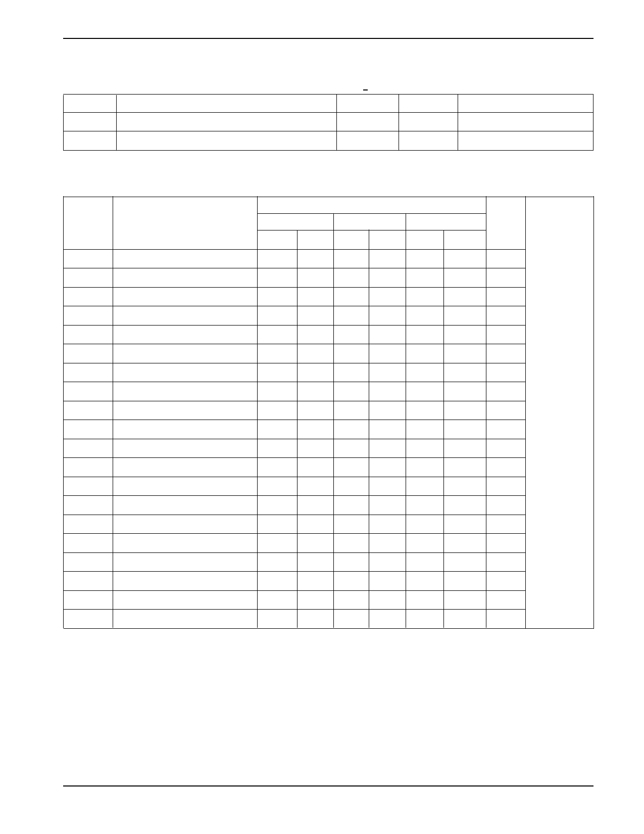
CAT25C11/03/05/09/17
PIN CAPACITANCE (1)
Applicable over recommended operating range from TA=25˚C, f=1.0 MHz, VCC=+5.0V (unless otherwise noted).
Symbol
Test Conditions
Max.
Units Conditions
COUT Output Capacitance (SO)
8
pF
VOUT=0V
CIN
Input Capacitance (CS, SCK, SI, WP, HOLD)
6
pF
VIN=0V
A.C. CHARACTERISTICS
SYMBOL PARAMETER
Limits
1.8V-6.0V 2.5V-6.0V
Min. Max. Min. Max.
4.5V-5.5V
Min. Max.
Test
UNITS Conditions
tSU
Data Setup Time
50
20
20
ns VIH = 2.4V
tH
Data Hold Time
50
20
20
ns CL = 100pF
tWH
SCK High Time
250
75
40
ns VOL = 0.8V
tWL
SCK Low Time
250
75
40
ns VOH = 2.0v
fSCK
tLZ
tRI(1)
tFI(1)
tHD
tCD
tWC(3)
Clock Frequency
HOLD to Output Low Z
Input Rise Time
Input Fall Time
HOLD Setup Time
HOLD Hold Time
Write Cycle Time
DC
1 DC
5 DC 10 MHz
50
50
50
ns
2
2
2
µs
CL = 50pF
2
2
2
µs
(note 2)
100
40
40
ns
100
40
40
ns CL = 100pF
10
5
5
ms
tV
Output Valid from Clock Low
250
75
40
ns
tHO
Output Hold Time
0
0
0
ns
tDIS
tHZ
tCS
tCSS
tCSH
tWPS
tCSH
Output Disable Time
HOLD to Output High Z
CS High Time
CS Setup Time
CS Hold Time
WP Setup Time
CS Hold Time
250
75
75
ns
150
50
50
ns
500
100
100
ns
500
100
100
ns
500
100
100
ns
150
50
50
ns
150
50
50
ns
(1) This parameter is tested initially and after a design or process change that affects the parameter.
(2) AC Test Conditions:
Input Pulse Voltages: 0.3VCC to 0.7VCC
Input rise and fall times: ≤10ns
Input and output reference voltages: 0.5VCC
Output load: current source IOL max/IOH max; CL = 50pF
(3) tWC is the time from the rising edge of CS after a valid write sequence to the end of the internal write cycle.
3
Doc. No. 1017, Rev. J
Share Link: 