S93VP462S-2.7T データシートの表示(PDF) - Summit Microelectronics
部品番号
コンポーネント説明
メーカー
S93VP462S-2.7T Datasheet PDF : 12 Pages
| |||
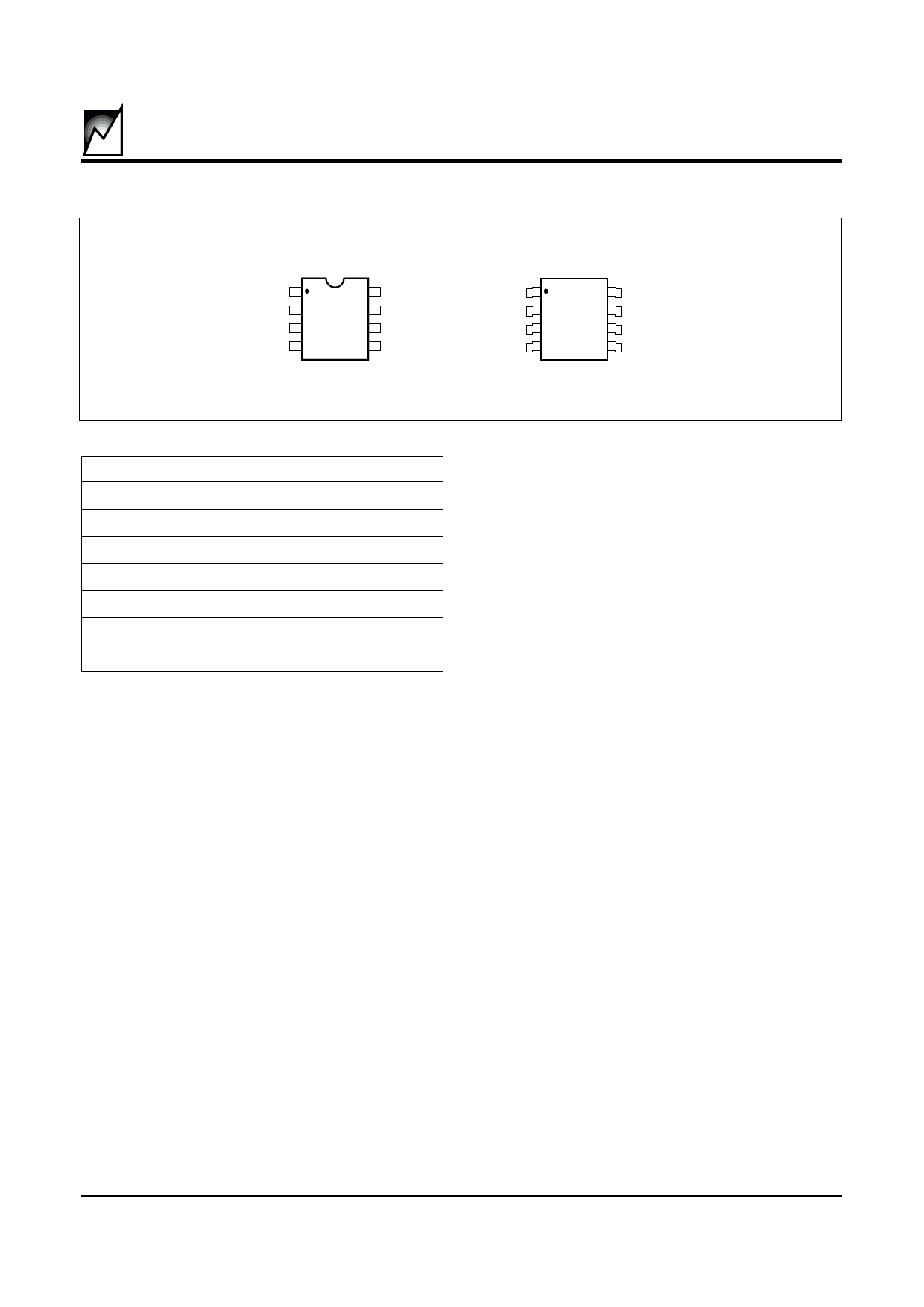
PIN CONFIGURATION
S93VP462/S93VP463
DIP Package (P)
CS 1
SK 2
DI 3
DO 4
8 VCC
7 NC
6 NC
5 GND
SOIC Package (S)
CS 1
SK 2
DI 3
DO 4
8 VCC
7 NC
6 NC
5 GND
2040 ILL1.0
PIN FUNCTIONS
Pin Name
CS
SK
DI
DO
VCC
GND
NC
Function
Chip Select
Clock Input
Serial Data Input
Serial Data Output
+2.7 to 6.0V Power Supply
Ground
No Connect
DEVICE OPERATION
WRITE LOCKOUT DESCRIPTION
The S93VP462/VP463 provides a precision internal
reset controller that ensures correct system operation
during brown-out and power-up/-down conditions.
During power-up, the write lockout remains active until
VCC reaches the VTRIP threshold. Write lockout will
continue to be driven for approximately 150 ms after VCC
reaches VTRIP. During power-down, write lockout will be
driven active when even VCC falls below VTRIP.
GENERAL OPERATION
The S93VP462/VP463 is a 1024-bit nonvolatile memory
intended for use with industry standard microproces-
sors. The S93VP463 is organized as X16, seven 9-bit
instructions control the reading, writing and erase
operations of the device. The S93VP462 is organized as
X8, seven 10-bit instructions control the reading, writing
and erase operations of the device. The device operates
on a single 3V or 5V supply and will generate on chip, the
high voltage required during any write operation.
Instructions, addresses, and write data are clocked into
the DI pin on the rising edge of the clock (SK). The DO
pin is normally in a high impedance state except when
reading data from the device, or when checking the
ready/busy status after a write operation.
The ready/busy status can be determined after the start
of a write operation by selecting the device (CS high) and
polling the DO pin; DO low indicates that the write
operation is not completed, while DO high indicates that
the device is ready for the next instruction. See the
Applications Aid section for detailed use of the ready
busy status.
The format for all instructions is: one start bit; two op
code bits and either six (x16) or seven (x8) address or
instruction bits.
2040-01 10/23/98
2
Share Link: 