UAA2077TS データシートの表示(PDF) - Philips Electronics
部品番号
コンポーネント説明
メーカー
UAA2077TS Datasheet PDF : 16 Pages
| |||
Philips Semiconductors
2 GHz image rejecting front-end
Preliminary specification
UAA2077TS
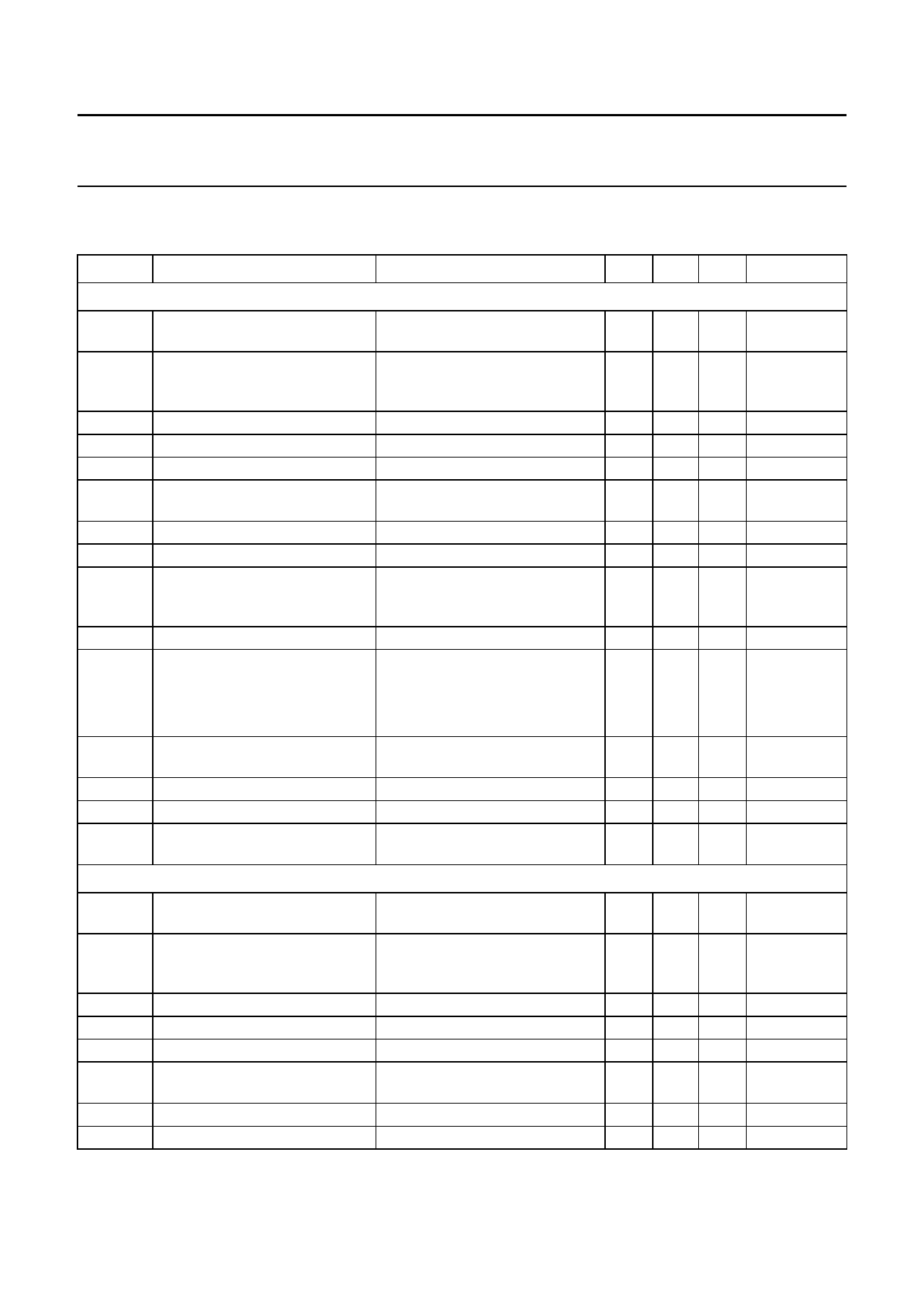
AC CHARACTERISTICS
VCC = 2.8 V; Tamb = 25 °C; fo(RX) = 200 MHz; unless otherwise specified.
SYMBOL
PARAMETER
CONDITIONS
MIN. TYP. MAX.
UNIT
Receive section (receive section enabled): DCS mode
Ri(RX)
Ci(RX)
fi(RX)
RLi(RX)
GCP(RX)
Grip
∆G/T
CP1RX
DES3
IP3RX
NFRX
ZL(RX)
RLo(RX)
fo(RX)
IR
RF input resistance (real part of balanced; at 1845 MHz
the parallel input impedance)
−
50 −
Ω
RF input capacitance (imaginary balanced; at 1845 MHz
part of the parallel input
impedance)
−
0.5 −
pF
RF input frequency
1805 −
1880 MHz
return loss on matched RF input balanced; note 1
10 15 −
dB
conversion power gain
RF inputs to IF outputs; note 1 20 23 26 dB
gain ripple as a function of RF over DCS frequency range;
frequency
note 1
−
−1 −1.5 dB/100 MHz
gain variation with temperature
−60 −30 −
mdB/K
1 dB compression point
referenced to RF input; note 1 −23.5 −20 −
dBm
input referred
3 dB desensitisation
interferer frequency offset is
3 MHz; useful signal is
−101 dBm; note 1
−25 −
−
dBm
3rd order intercept point
referenced to RF input; note 1 −15 −12 −
dBm
overall noise figure
RF inputs to IF outputs; note 1
normal case
−
3.5 4.2 dB
worse case for LO input, power −
and VCC
typical application IF output load balanced; note 1
−
impedance
−
4.4 dB
1000 −
Ω
return loss on matched IF output note 1
10 15 −
dB
IF frequency range
rejection of image frequency
fRF > fLO
−
fRF > fLO; fRF is the frequency of 30
the wanted signal; note 1
200 −
38 −
MHz
dB
Receive section (receive section enabled): PCS mode
Ri(RX)
Ci(RX)
fi(RX)
RLi(RX)
GCP(RX)
Grip
∆G/T
CP1RX
RF input resistance (real part of balanced; at 1960 MHz
the parallel input impedance)
RF input capacitance (imaginary balanced; at 1960 MHz
part of the parallel input
impedance)
RF input frequency
return loss on matched RF input balanced; note 1
conversion power gain
RF inputs to IF outputs; note 1
gain ripple as a function of
RF frequency
over PCS frequency range;
note 1
gain variation with temperature
1 dB compression point
referenced to RF input; note 1
−
tbf −
Ω
−
tbf −
pF
1930 −
10 15
−
22
−
−1
1 990
−
−
−
MHz
dB
dB
dB/100 MHz
−
−30 −
mdB/K
−
−20 −
dBm
2000 Apr 17
7
Share Link: 