M29F002BB データシートの表示(PDF) - STMicroelectronics
部品番号
コンポーネント説明
メーカー
M29F002BB Datasheet PDF : 22 Pages
| |||
M29F002BT, M29F002BB, M29F002BNT, M29F002BNB
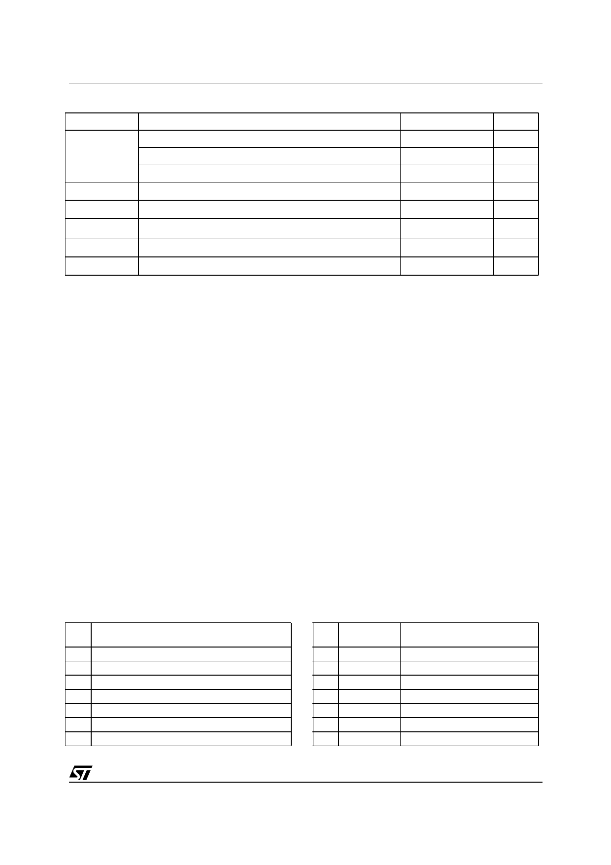
Table 2. Absolute Maximum Ratings (1)
Symbol
Parameter
Value
Unit
Ambient Operating Temperature (Temperature Range Option 1)
0 to 70
°C
TA
Ambient Operating Temperature (Temperature Range Option 6)
–40 to 85
°C
Ambient Operating Temperature (Temperature Range Option 3)
–40 to 125
°C
TBIAS
Temperature Under Bias
–50 to 125
°C
TSTG
Storage Temperature
–65 to 150
°C
VIO (2)
Input or Output Voltage
–0.6 to 6
V
VCC
Supply Voltage
–0.6 to 6
V
VID
Identification Voltage
–0.6 to 13.5
V
Note: 1. Except for the rating "Operating Temperature Range", stresses above those listed in the Table "Absolute Maximum Ratings" may
cause permanent damage to the device. These are stress ratings only and operation of the device at these or any other conditions
above those indicated in the Operating sections of this specification is not implied. Exposure to Absolute Maximum Rating condi-
tions for extended periods may affect device reliability. Refer also to the STMicroelectronics SURE Program and other relevant qual-
ity documents.
2. Minimum Voltage may undershoot to –2V during transition and for less than 20ns during transitions.
SUMMARY DESCRIPTION
The M29F002B is a 2 Mbit (256Kb x8) non-volatile
memory that can be read, erased and repro-
grammed. These operations can be performed us-
ing a single 5V supply. On power-up the memory
defaults to its Read mode where it can be read in
the same way as a ROM or EPROM. The
M29F002B is fully backward compatible with the
M29F002.
The memory is divided into blocks that can be
erased independently so it is possible to preserve
valid data while old data is erased. Each block can
be protected independently to prevent accidental
Program or Erase commands from modifying the
memory. Program and Erase commands are writ-
ten to the Command Interface of the memory. An
on-chip Program/Erase Controller simplifies the
process of programming or erasing the memory by
taking care of all of the special operations that are
required to update the memory contents. The end
Table 3. Top Boot Block Addresses,
M29F002BT, M29F002BNT
#
Size
(Kbytes)
Address Range
6
16
3C000h-3FFFFh
5
8
3A000h-3BFFFh
4
8
38000h-39FFFh
3
32
30000h-37FFFh
2
64
20000h-2FFFFh
1
64
10000h-1FFFFh
0
64
00000h-0FFFFh
of a program or erase operation can be detected
and any error conditions identified. The command
set required to control the memory is consistent
with JEDEC standards.
The blocks in the memory are asymmetrically ar-
ranged, see Tables 3A and 3B, Block Addresses.
The first or last 64 Kbytes have been divided into
four additional blocks. The 16 Kbyte Boot Block
can be used for small initialization code to start the
microprocessor, the two 8 Kbyte Parameter
Blocks can be used for parameter storage and the
remaining 32K is a small Main Block where the ap-
plication may be stored.
Chip Enable, Output Enable and Write Enable sig-
nals control the bus operation of the memory.
They allow simple connection to most micropro-
cessors, often without additional logic.
The memory is offered in TSOP32 (8 x 20mm),
PLCC32 and PDIP packages and it is supplied
with all the bits erased (set to ’1’).
Table 4. Bottom Boot Block Addresses,
M29F002BB
#
Size
(Kbytes)
Address Range
6
64
30000h-3FFFFh
5
64
20000h-2FFFFh
4
64
10000h-1FFFFh
3
32
08000h-0FFFFh
2
8
06000h-07FFFh
1
8
04000h-05FFFh
0
16
00000h-03FFFh
3/22
Share Link: 