M29F002BB データシートの表示(PDF) - STMicroelectronics
部品番号
コンポーネント説明
メーカー
M29F002BB Datasheet PDF : 22 Pages
| |||
M29F002BT, M29F002BB, M29F002BNT, M29F002BNB
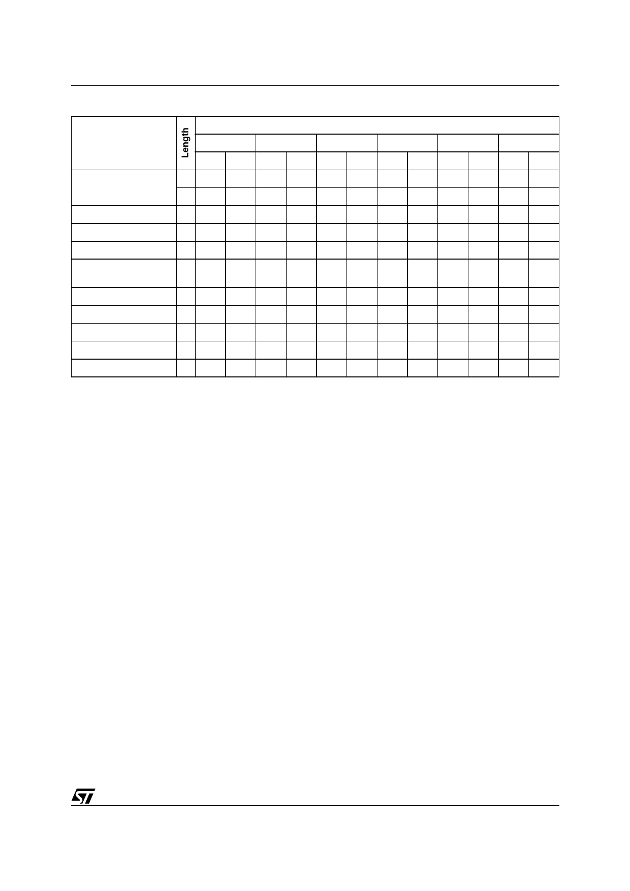
Table 6. Commands
Bus Write Operations
Command
1st
2nd
3rd
4th
5th
6th
Addr Data Addr Data Addr Data Addr Data Addr Data Addr Data
Read/Reset
1 X F0
3 555 AA 2AA 55 X F0
Auto Select
3 555 AA 2AA 55 555 90
Program
4 555 AA 2AA 55 555 A0 PA PD
Unlock Bypass
3 555 AA 2AA 55 555 20
Unlock Bypass
Program
2 X A0 PA PD
Unlock Bypass Reset 2 X 90 X 00
Chip Erase
6 555 AA 2AA 55 555 80 555 AA 2AA 55 555 10
Block Erase
6+ 555 AA 2AA 55 555 80 555 AA 2AA 55 BA 30
Erase Suspend
1 X B0
Erase Resume
1 X 30
Note: X Don’t Care, PA Program Address, PD Program Data, BA Any address in the Block.
All values in the table are in hexadecimal.
The Command Interface only uses address bits A0-A10 to verify the commands, the upper address bits are Don’t Care.
Read/Reset. After a Read/Reset command, read the memory as normal until another command is issued.
Auto Select. After an Auto Select command, read Manufacturer ID, Device ID or Block Protection Status.
Program, Unlock Bypass Program, Chip Erase, Block Erase. After these commands read the Status Register until the Program/Erase
Controller completes and the memory returns to Read Mode. Add additional Blocks during Block Erase Command with additional Bus Write
Operations until the Timeout Bit is set.
Unlock Bypass. After the Unlock Bypass command issue Unlock Bypass Program or Unlock Bypass Reset commands.
Unlock Bypass Reset. After the Unlock Bypass Reset command read the memory as normal until another command is issued.
Erase Suspend. After the Erase Suspend command read non-erasing memory blocks as normal, issue Auto Select and Program commands
on non-erasing blocks as normal.
Erase Resume. After the Erase Resume command the suspended Erase operation resumes, read the Status Register until the Program/
Erase Controller completes and the memory returns to Read Mode.
Unlock Bypass Reset Command. The Unlock
Bypass Reset command can be used to return to
Read/Reset mode from Unlock Bypass Mode.
Two Bus Write operations are required to issue the
Unlock Bypass Reset command.
Chip Erase Command. The Chip Erase com-
mand can be used to erase the entire chip. Six Bus
Write operations are required to issue the Chip
Erase Command and start the Program/Erase
Controller.
If any blocks are protected then these are ignored
and all the other blocks are erased. If all of the
blocks are protected the Chip Erase operation ap-
pears to start but will terminate within about 100µs,
leaving the data unchanged. No error condition is
given when protected blocks are ignored.
During the erase operation the memory will ignore
all commands. It is not possible to issue any com-
mand to abort the operation. Typical chip erase
times are given in Table 7. All Bus Read opera-
tions during the Chip Erase operation will output
the Status Register on the Data Inputs/Outputs.
See the section on the Status Register for more
details.
After the Chip Erase operation has completed the
memory will return to the Read Mode, unless an
error has occurred. When an error occurs the
memory will continue to output the Status Regis-
ter. A Read/Reset command must be issued to re-
set the error condition and return to Read Mode.
The Chip Erase Command sets all of the bits in un-
protected blocks of the memory to ’1’. All previous
data is lost.
7/22
Share Link: 