LA4192 データシートの表示(PDF) - SANYO -> Panasonic
部品番号
コンポーネント説明
メーカー
LA4192 Datasheet PDF : 11 Pages
| |||
LA4192
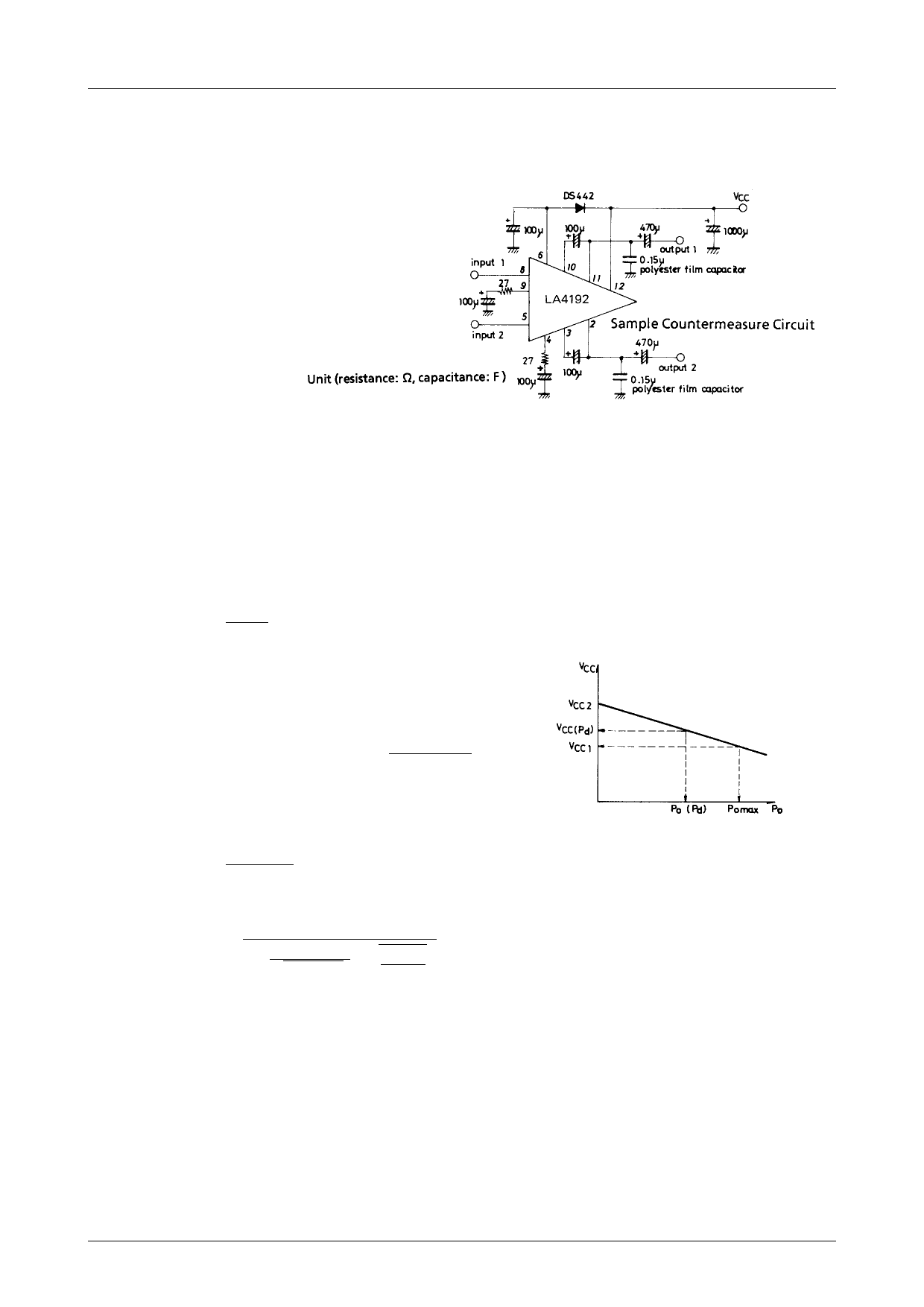
• Caution for LA4192 in sets
When LA4192 is used in a set and driven by AC mains, switching the motor on as shwon below, causes instantaneous
lowering of the power supply voltage, depending on the transformer regulation and other conditions.
Ripple noises are sometimes generated in the speakers or headphones. The following can be used to prevent such prob-
lems.
1. Connect a diode (a rectifier diode with an average
rectified current IO=100 to 200mA) across pins 6
and 12 of LA4192, and have pin 6 potential closely
follow power supply voltage variations. In a steady
state, this diode will be cut off.
2. Use large enough capacitance capacitors for the
power supply to suppress supply votage variations
caused when the motor is switched on.
• Heat sink design
As the package is basically heat-dissipated by utilizing a copper foil section of the printed circuit board, the area of
copper foil in the vicinity of the IC heat dissipating plate should be made as broad in area as possible when designing the
printed circuit board. For the sample printed pattern shown earlier, providing copper coil where indicated by the broken
lines will considerably enhance heat sinking. Power consumption (Pd) can be increased depending on power supply
voltage and load conditions. Use of a heat sink in conjunction with the printed circuit board is recommended. Described
below are formulas to provide guidelines for Pd (for 2 channels) under various conditions of usage. For AC power
supplies, it is preferable to take actual measurements at the transformer of sets. For bridge amplifier, simply use 1/2 of
employed loads in computations.
1) DC power supply
Pd max=
VCC2
π2RL
+ICCO · VCC (for 2 channels) .............................................. (1)
2) AC power supply
VCC2 :
VCC (Pd) :
VCC1 :
Power supply voltage at no signal
Power supply voltage at Pd max
Power supply voltage at maximum output
r:
ICCO :
Voltage regulation VCC2–VCC1
VCC1
Quiescent current
Power supply voltage variation
Pd max=
VCC(Pd)2
π2RL
+ICCO · VCC (Pd) (for 2 channels) ............................... (2)
where
VCC (Pd)=
1+
(1+r) VCC1
√ r · VCC1
√2 · π · RL
×
RL
PO max
Sample heat sink mounting
Prepare a heat sink as shown on the next page. It is configured to be able to dissipate heat both from the IC plastic surface
and its fins. Solder it on to the printed circuit board. Refer to the Pd – Ta characteristics for size of heat sink. Solderable
copper or steel are preferable. Silicone grease is recommended for application to the IC plastic surface to lower its
thermal resistance with the heat sink.
No.919–6/11
Share Link: 