CXA3541N データシートの表示(PDF) - Sony Semiconductor
部品番号
コンポーネント説明
メーカー
CXA3541N Datasheet PDF : 17 Pages
| |||
CXA3541N
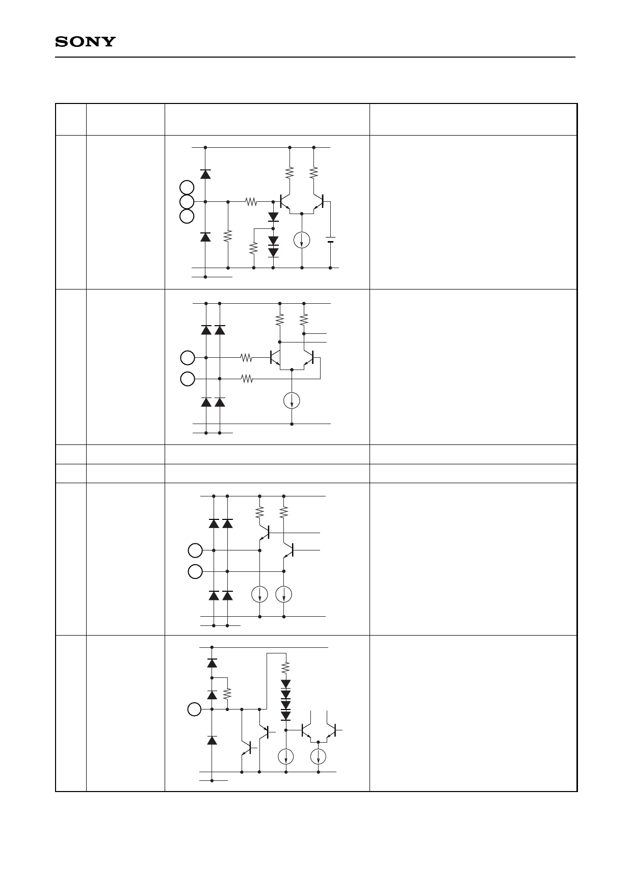
Pin Description
Pin
No.
Symbol
1 SCLK
2 SDATA
11 SDEN
Equivalent circuit
VCC
Description
1
7.5k
2
11
14k
VEE
Serial control signal input.
2Vf
GND
VCC
3 WDX
4 WDY
5 VCC
6 GND
7 RDY
8 RDX
100
3
4
100
Differential P-ECL write data input.
GND
VEE
5V power supply.
Ground.
VCC
100
7
Read amplifier output with coupling
capacitors.
8
High impedance in the write mode.
1.8mA
GND
VEE
VCC
9 FLT/SE/BHV
9
VEE
Head unsafe detection output.
Servo bank write enable input.
Buffered head voltage output.
GND
–3–
Share Link: 