MC145201 データシートの表示(PDF) - Motorola => Freescale
部品番号
コンポーネント説明
メーカー
MC145201 Datasheet PDF : 23 Pages
| |||
LOOP SPECIFICATIONS (VDD = VCC = 4.5 to 5.5 V unless otherwise indicated, TA = – 40 to + 85°C)
Symbol
Parameter
Vin Input Voltage Range, fin
fref Input Frequency, REFin
Externally Driven in
Reference Mode
fXTAL Crystal Frequency, Crystal Mode
Test Condition
500 MHz ≤ fin ≤ 2000 MHz
MC145200
MC145201
Vin ≥ 400 mV p–p
Vin ≥ 1 V p–p
Vin ≥ 400 mV p–p
Vin ≥ 1 V p–p
C1 ≤ 30 pF, C2 ≤ 30 pF, Includes Stray
Capacitance
Figure
No.
7
8
9
Guaranteed
Operating Range
Min
Max
200
1500
13
27
6*
27
12
27
4.5*
27
2
15
Unit
mV p–p
MHz
MHz
fout Output Frequency, REFout
CL = 30 pF
f
Operating Frequency of the Phase Detectors
10, 12
dc
dc
10
MHz
2
MHz
tw Output Pulse Width, LD, φR, and
φV, — MC145200, MC145201
fR in Phase with fV, CL = 50 pF,
VPD = 5.5 V, VDD = VCC = 5.0 V
tTLH, Output Transition Times, LD, φV, and
tTHL φR — MC145201
CL = 50 pF, VPD = 5.5 V,
VDD = VCC = 5.0 V
Cin Input Capacitance
fin
REFin
*If lower frequency is desired, use wave shaping or higher amplitude sinusoidal signal.
11, 12
17
85
ns
11, 12
—
65
ns
—
TBD
pF
—
5
SINE WAVE
GENERATOR
50 Ω*
1000 pF
fin OUTPUT A
1000 pF
Vin
fin
DEVICE
UNDER
TEST
VCC GND VDD
*Characteristic Impedance
TEST
POINT
(fv)
V+
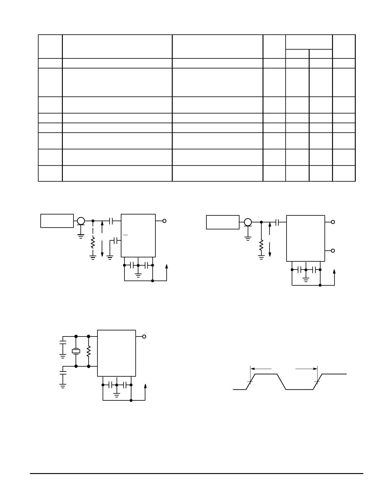
Figure 7. Test Circuit
SINE WAVE
GENERATOR
0.01 µF
REFin OUTPUT A
DEVICE
TEST
POINT
(fR)
Vin
50 Ω
UNDER
TEST
REFout
VCC GND VDD
TEST
POINT
V+
Figure 8. Test Circuit–Reference Mode
TEST
REFin OUTPUT A
POINT
C1
DEVICE
(fR)
UNDER
TEST
REFout
C2
VCC GND VDD
V+
Figure 9. Test Circuit–Crystal Mode
REFout
1/f REFout
50%
Figure 10. Switching Waveform
MC145200•MC145201
6
MOTOROLA
Share Link: 