HV832MG データシートの表示(PDF) - Supertex Inc
部品番号
コンポーネント説明
メーカー
HV832MG Datasheet PDF : 6 Pages
| |||
HV832
HV832
Dual High Voltage, Low Noise EL Lamp Driver
Features
❏ 8-pin dual EL driver IC
❏ Input control for lamp selection
❏ Split supply capability
❏ Patented output timing
❏ One minature inductor to power both lamps
❏ 150nA shutdown current
❏ Wide input voltage range (2.0V to 5.0V)
❏ Output voltage regulation
❏ No SCR output
Applications
❏ Dual display cell phones
❏ Keypad and LCD backlighting
❏ Dual segment lamps
❏ Handheld wireless communication devices
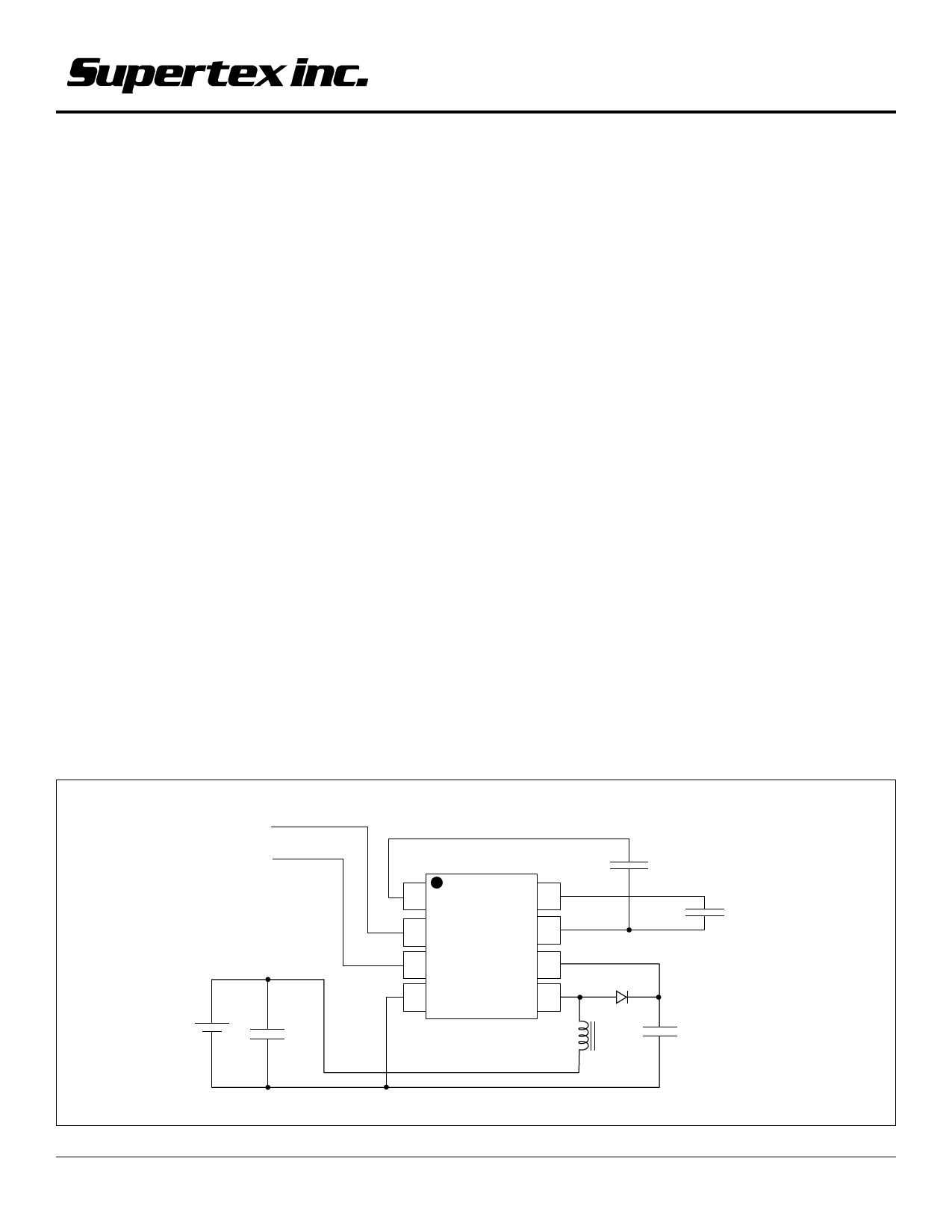
Typical Application
General Description
The Supertex HV832 is a high voltage driver designed for driving
two EL lamps with a combined area of 3.5 square inches. The
input supply voltage range is from 2.0V to 5.0V. The device is
designed to reduce the amount of audible noise emitted by the
lamp. The device uses a single inductor and a minimum number
of passive components. The nominal regulated output voltage
that is applied to the EL lamp is ±90V.
The HV832 has an internal oscillator, a switching MOSFET, and
two high voltage EL lamp drivers. The frequency for the switching
MOSFET is set at 51KHz nominal. The EL lamp driver frequency
is set by dividing the MOSFET switching frequency by 128. An
external inductor is connected between the LX and VDD pins or
VIN for split supply applications. A 0.001 to 0.01µF, 100V
capacitor is connected between CS and Ground. The EL lamps
are connected between EL1 to Com and EL2 to Com.
An input control pin is available to select various modes of the
device. Each logic pulse applied to the control pin will cause the
device to change to the next mode. The sequence for the modes
is: (1) EL1 on only, (2) EL2 on only, (3) both EL1 and EL2 on, and
(4) device shuts down. During power up of the device, the mode
will default to shut down.
The switching MOSFET charges the external inductor and
discharges it into the capacitor at Cs. The voltage at CS will start
to increase. Once the voltage at Cs reaches a nominal value of
90V, the switching MOSFET is turned off to conserve power. The
outputs EL1 to Com and EL2 to Com are configured as H bridges
EL1/EL2 and Com are switching in opposite states to achieve
180V across the EL lamp.
VDD
Logic Input Pulse
+
VIN _
CIN
1 EL1
2 VDD
EL2 8
Com 7
3 Control
CS 6
4 GND
LX 5
HV832MG
EL Lamp 1
EL Lamp 2
LX
CS
12/13/01
Supertex Inc. does not recommend the use of its products in life support applications and will not knowingly sell its products for use in such applications unless it receives an adequate "products liability
indemnification insurance agreement." Supertex does not assume responsibility for use of devices described and limits its liability to the replacement of devices determined to be defective due to
workmanship. No responsibility is assumed for possible omissions or inaccuracies. Circuitry and s1pecifications are subject to change without notice. For the latest product specifications, refer to the
Supertex website: http://www.supertex.com. For complete liability information on all Supertex products, refer to the most current databook or to the Legal/Disclaimer page on the Supertex website.
Share Link: 