24C02A データシートの表示(PDF) - Microchip Technology
部品番号
コンポーネント説明
メーカー
24C02A Datasheet PDF : 12 Pages
| |||
24C01A/02A/04A
1K/2K/4K 5.0V I2C™ Serial EEPROMs
FEATURES
• Low power CMOS technology
• Hardware write protect
• Two wire serial interface bus, I2C™ compatible
• 5.0V only operation
• Self-timed write cycle (including auto-erase)
• Page-write buffer
• 1ms write cycle time for single byte
• 1,000,000 Erase/Write cycles guaranteed
• Data retention >200 years
• 8-pin DIP/SOIC packages
• Available for extended temperature ranges
- Commercial (C):
- Industrial (I):
- Automotive (E):
0˚C to +70˚C
-40˚C to +85˚C
-40˚C to +125˚C
DESCRIPTION
The Microchip Technology Inc. 24C01A/02A/04A is a
1K/2K/4K bit Electrically Erasable PROM. The device
is organized as shown, with a standard two wire serial
interface. Advanced CMOS technology allows a signif-
icant reduction in power over NMOS serial devices. A
special feature in the 24C02A and 24C04A provides
hardware write protection for the upper half of the block.
The 24C01A and 24C02A have a page write capability
of two bytes and the 24C04A has a page length of eight
bytes. Up to eight 24C01A or 24C02A devices and up
to four 24C04A devices may be connected to the same
two wire bus.
This device offers fast (1ms) byte write and
extended (-40°C to 125°C) temperature operation. It
is recommended that all other applications use
Microchip’s 24LCXXB.
Organization
Write Protect
Page Write
Buffer
24C01A
128 x 8
None
2 Bytes
24C02A
258 x 8
080-0FF
2 Bytes
24C04A
2 x 256 x 8
100-1FF
8 Bytes
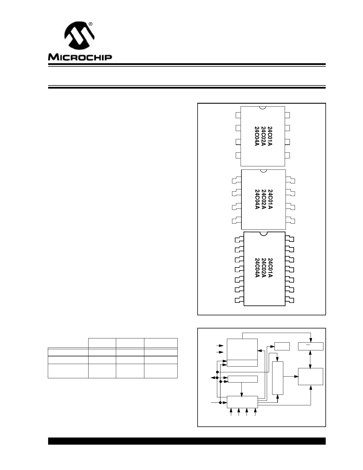
PACKAGE TYPES
DIP
A0 1
A1 2
A2 3
VSS 4
8-lead
SOIC A0
1
A1
2
A2
3
VSS
4
14-lead
SOIC
NC
1
A0
2
A1
3
NC
4
A2
5
VSS
6
NC
7
* “TEST” pin in 24C01A
BLOCK DIAGRAM
Vcc
Vss
SDA
Data
Buffer
(FIFO)
Data Reg.
Slave Addr.
Control
SCL
Logic
I2C is a trademark of Philips Corporation.
A0 A1 A2 WP
© 1996 Microchip Technology Inc.
This document was created with FrameMaker 4 0 4
8 VCC
7 WP*
6 SCL
5 SDA
8
VCC
7
WP*
6
SCL
5
SDA
14
NC
13
VCC
12
WP
11
NC
10
SCL
9
SDA
8
NC
Vpp
R/W Amp
AP
do
di
rn
et
se
A0 to
A7
sr
Memory
Array
Increment
A8
DS11183D-page 1
Share Link: 