24LC025T-/ST データシートの表示(PDF) - Microchip Technology
部品番号
コンポーネント説明
メーカー
24LC025T-/ST Datasheet PDF : 12 Pages
| |||
24LC024/24LC025
4.0 BUS CHARACTERISTICS
The following bus protocol has been defined:
• Data transfer may be initiated only when the bus is
not busy.
• During data transfer, the data line must remain
stable whenever the clock line is HIGH. Changes
in the data line while the clock line is HIGH will be
interpreted as a START or STOP condition.
Accordingly, the following bus conditions have been
defined (Figure 4-1).
4.1 Bus not Busy (A)
Both data and clock lines remain HIGH.
4.2 Start Data Transfer (B)
A HIGH to LOW transition of the SDA line while the
clock (SCL) is HIGH determines a START condition. All
commands must be preceded by a START condition.
4.3 Stop Data Transfer (C)
A LOW to HIGH transition of the SDA line while the
clock (SCL) is HIGH determines a STOP condition. All
operations must be ended with a STOP condition.
4.4 Data Valid (D)
The state of the data line represents valid data when,
after a START condition, the data line is stable for the
duration of the HIGH period of the clock signal.
The data on the line must be changed during the LOW
period of the clock signal. There is one bit of data per
clock pulse.
Each data transfer is initiated with a START condition
and terminated with a STOP condition. The number of
the data bytes transferred between the START and
STOP conditions is determined by the master device
and is theoretically unlimited, although only the last six-
teen will be stored when doing a write operation. When
an overwrite does occur it will replace data in a first in
first out fashion.
4.5 Acknowledge
Each receiving device, when addressed, is required to
generate an acknowledge after the reception of each
byte. The master device must generate an extra clock
pulse which is associated with this acknowledge bit.
Note:
The 24LC024/24LC025 does not generate
any acknowledge bits if an internal pro-
gramming cycle is in progress.
The device that acknowledges has to pull down the
SDA line during the acknowledge clock pulse in such a
way that the SDA line is stable LOW during the HIGH
period of the acknowledge related clock pulse. Of
course, setup and hold times must be taken into
account. A master must signal an end of data to the
slave by not generating an acknowledge bit on the last
byte that has been clocked out of the slave. In this case,
the slave must leave the data line HIGH to enable the
master to generate the STOP condition (Figure 4-2).
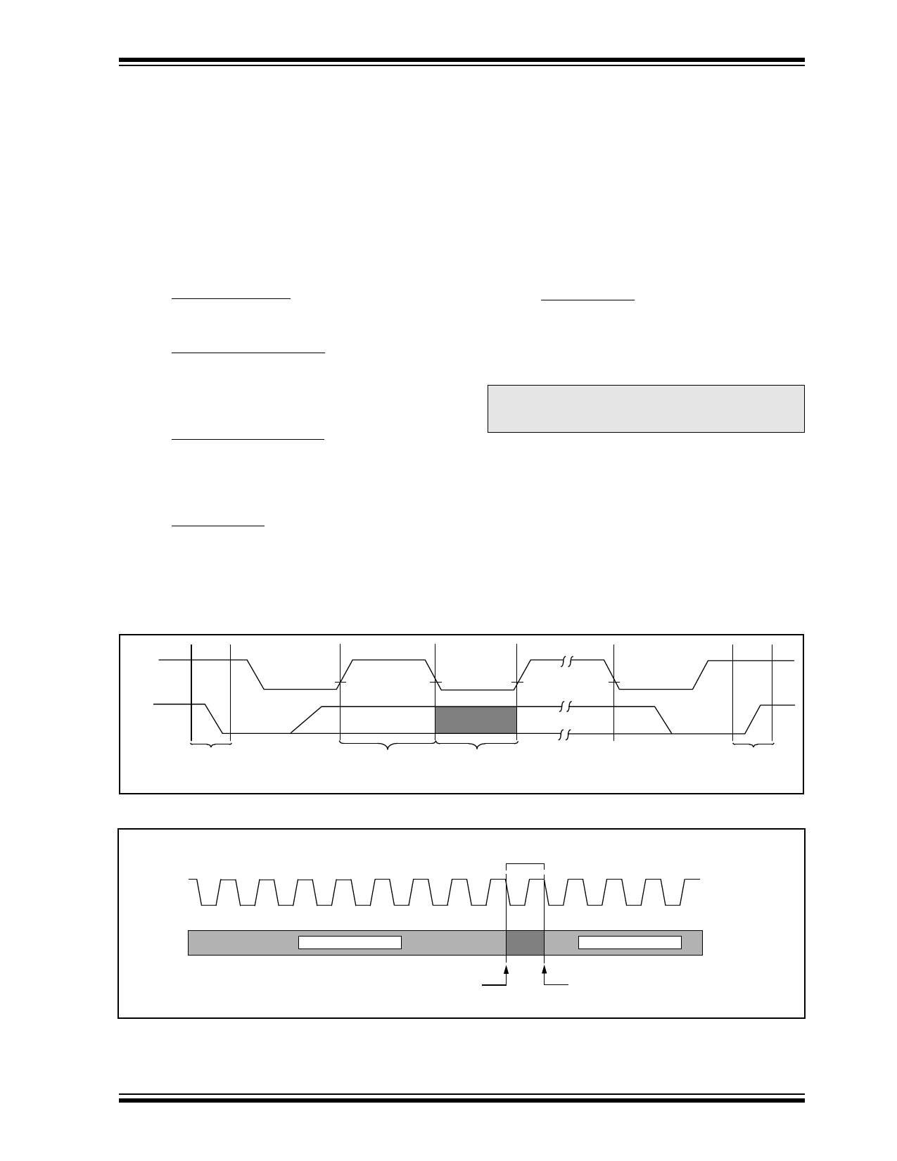
FIGURE 4-1: DATA TRANSFER SEQUENCE ON THE SERIAL BUS CHARACTERISTICS
SCL (A) (B)
(C)
(D)
(C) (A)
SDA
START
CONDITION
ADDRESS OR
ACKNOWLEDGE
VALID
DATA
ALLOWED
TO CHANGE
FIGURE 4-2: ACKNOWLEDGE TIMING
Acknowledge
Bit
SCL
12 345678 9 123
STOP
CONDITION
SDA
Data from transmitter
Transmitter must release the SDA line at this point
allowing the Receiver to pull the SDA line low to
acknowledge the previous eight bits of data.
Data from transmitter
Receiver must release the SDA line at this point
so the Transmitter can continue sending data.
© 1997 Microchip Technology Inc.
Preliminary
DS21210A-page 5
Share Link: 