24C64 データシートの表示(PDF) - Microchip Technology
部品番号
コンポーネント説明
メーカー
24C64 Datasheet PDF : 12 Pages
| |||
25AA640/25LC640/25C640
1.0 ELECTRICAL
CHARACTERISTICS
1.1 Maximum Ratings*
Vcc ...................................................................................7.0V
All inputs and outputs w.r.t. Vss.................. -0.6V to Vcc+1.0V
Storage temperature ....................................... -65˚C to 150˚C
Ambient temperature under bias..................... -65˚C to 125˚C
Soldering temperature of leads (10 seconds) ............. +300˚C
ESD protection on all pins.................................................4kV
*Notice: Stresses above those listed under ‘Maximum ratings’ may
cause permanent damage to the device. This is a stress rating only and
functional operation of the device at those or any other conditions
above those indicated in the operational listings of this specification is
not implied. Exposure to maximum rating conditions for an extended
period of time may affect device reliability
TABLE 1-1: PIN FUNCTION TABLE
Name
Function
CS
SO
SI
SCK
WP
VSS
VCC
HOLD
Chip Select Input
Serial Data Output
Serial Data Input
Serial Clock Input
Write Protect Pin
Ground
Supply Voltage
Hold Input
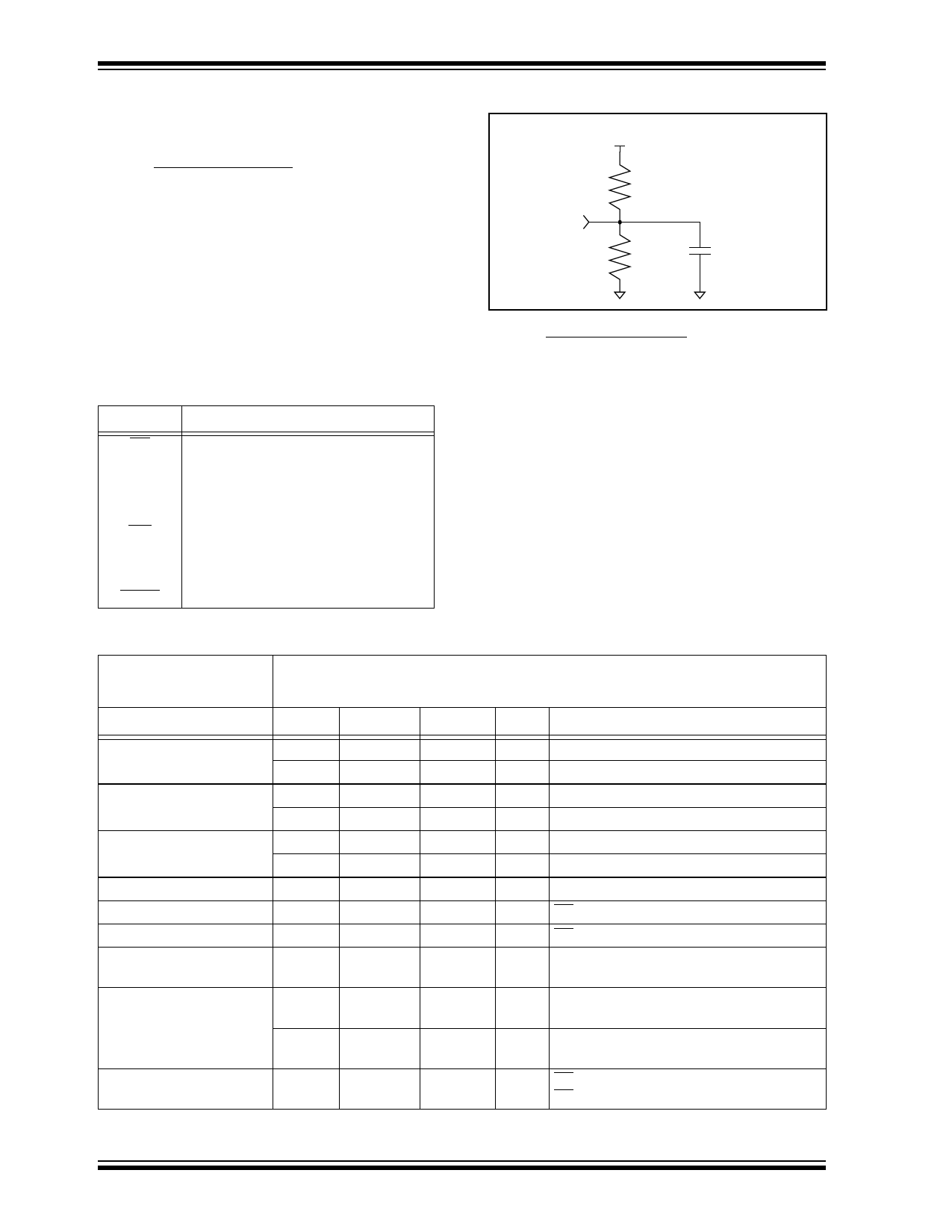
FIGURE 1-1: AC TEST CIRCUIT
VCC
2.25 K
SO
1.8 K
100 pF
1.2 AC Test Conditions
AC Waveform:
VLO = 0.2V
VHI = VCC - 0.2V
(Note 1)
VHI = 4.0V
(Note 2)
Timing Measurement Reference Level
Input
0.5 VCC
Output
0.5 VCC
Note 1: For VCC ≤ 4.0V
2: For VCC > 4.0V
TABLE 1-2: DC CHARACTERISTICS
All parameters apply over the Commercial (C): Tamb = 0°C to +70°C
specified operating ranges Industrial (I):
Tamb = -40°C to +85°C
unless otherwise noted.
Automotive (E): Tamb = -40°C to +125°C
VCC = 1.8V to 5.5V
VCC = 1.8V to 5.5V
VCC = 4.5V to 5.5V (25C640 only)
Parameter
Symbol
Min
Max Units
Test Conditions
High level input voltage
VIH1
2.0
VCC+1
V
VIH2
0.7 VCC
VCC+1
V
VIL1
-0.3
0.8
V
Low level input voltage
VIL2
-0.3
0.3 VCC
V
VOL
—
Low level output voltage
VOL
—
0.4
V
0.2
V
High level output voltage
VOH
VCC -0.5
—
V
Input leakage current
ILI
-10
10
µA
Output leakage current
ILO
-10
10
µA
Internal Capacitance
CINT
—
(all inputs and outputs)
7
pF
Operating Current
ICC Read
—
—
ICC Write
—
—
1
mA
500
µA
5
mA
3
mA
Standby Current
ICCS
—
—
5
µA
1
µA
Note: This parameter is periodically sampled and not 100% tested.
VCC ≥ 2.7V (Note)
VCC< 2.7V (Note)
VCC ≥ 2.7V (Note)
VCC < 2.7V (Note)
IOL = 2.1 mA
IOL = 1.0 mA, VCC < 2.5V
IOH =-400 µA
CS = VCC, VIN = VSS TO VCC
CS = VCC, VOUT = VSS TO VCC
TAMB = 25˚C, CLK = 1.0 MHz,
VCC = 5.0V (Note)
VCC = 5.5V; FCLK=3.0 MHz; SO = Open
VCC = 2.5V; FCLK=2.0 MHz; SO = Open
VCC= 5.5V
VCC = 2.5V
CS = Vcc = 5.5V, Inputs tied to VCC or VSS
CS = Vcc = 2.5V, Inputs tied to VCC or VSS
DS21223A-page 2
Preliminary
© 1997 Microchip Technology Inc.
Share Link: 