24WC16 データシートの表示(PDF) - Catalyst Semiconductor => Onsemi
部品番号
コンポーネント説明
メーカー
24WC16 Datasheet PDF : 10 Pages
| |||
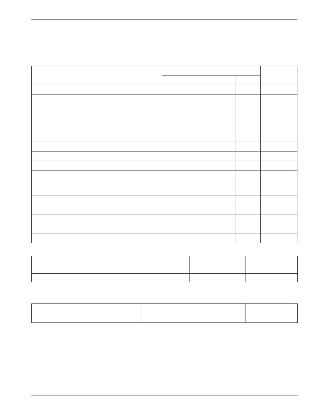
CAT24WC01/02/04/08/16
A.C. CHARACTERISTICS
VCC = +1.8V to +6.0V, unless otherwise specified.
Read & Write Cycle Limits
Symbol
FSCL
TI(1)
tAA
tBUF(1)
tHD:STA
tLOW
tHIGH
tSU:STA
tHD:DAT
tSU:DAT
tR(1)
tF(1)
tSU:STO
tDH
Parameter
Clock Frequency
Noise Suppression Time
Constant at SCL, SDA Inputs
SCL Low to SDA Data Out
and ACK Out
Time the Bus Must be Free Before
a New Transmission Can Start
Start Condition Hold Time
Clock Low Period
Clock High Period
Start Condition Setup Time
(for a Repeated Start Condition)
Data In Hold Time
Data In Setup Time
SDA and SCL Rise Time
SDA and SCL Fall Time
Stop Condition Setup Time
Data Out Hold Time
1.8V-6.0V, 2.5V-6.0V 4.5V-5.5V
Min. Max. Min. Max.
100
400
200
200
3.5
1
4.7
1.2
4
0.6
4.7
1.2
4
0.6
4.7
0.6
0
0
50
50
1
0.3
300
300
4
0.6
100
100
Power-Up Timing(1)(2)
Symbol
tPUR
tPUW
Parameter
Power-up to Read Operation
Power-up to Write Operation
Max.
1
1
Units
kHz
ns
µs
µs
µs
µs
µs
µs
ns
ns
µs
ns
µs
ns
Units
ms
ms
Write Cycle Limits
Symbol
Parameter
tWR
Write Cycle Time
Min.
Typ.
Max
10
Units
ms
The write cycle time is the time from a valid stop
condition of a write sequence to the end of the internal
program/erase cycle. During the write cycle, the bus
interface circuits are disabled, SDA is allowed to remain
high, and the device does not respond to its slave
address.
Note:
(1) This parameter is tested initially and after a design or process change that affects the parameter.
(2) tPUR and tPUW are the delays required from the time VCC is stable until the specified operation can be initiated.
3
Doc. No. 1022, Rev. J
Share Link: 