25AA040A データシートの表示(PDF) - Microchip Technology
部品番号
コンポーネント説明
メーカー
25AA040A Datasheet PDF : 38 Pages
| |||
25AA040A/25LC040A
2.6 Write Status Register Instruction
(WRSR)
The Write Status Register instruction (WRSR) allows the
user to write to the nonvolatile bits in the STATUS regis-
ter as shown in Table 2-2. See Figure 2-7 for the WRSR
timing sequence. Four levels of protection for the array
are selectable by writing to the appropriate bits in the
STATUS register. The user has the ability to write-protect
none, one, two or all four of the segments of the array as
shown in Table 2-3.
TABLE 2-3:
BP1
0
0
1
1
ARRAY PROTECTION
BP0
Array Addresses
Write-Protected
0
none
1
upper 1/4
(180h-1FFh)
0
upper 1/2
(100h-1FFh)
1
all
(000h-1FFh)
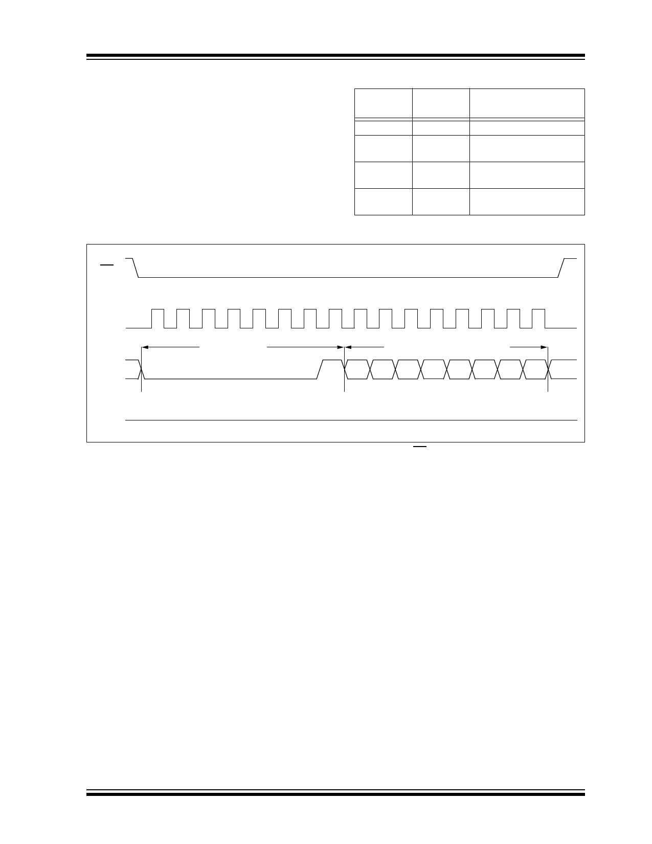
FIGURE 2-7:
WRITE STATUS REGISTER TIMING SEQUENCE (WRSR)
CS
SCK
SI
0 1 2 3 4 5 6 7 8 9 10 11 12 13 14 15
Instruction
Data to STATUS Register
0 00 00 0 01 7 6 54 3 2 10
High-Impedance
SO
Note: An internal write cycle (TWC) is initiated on the rising edge of CS after a valid write STATUS register
sequence.
2003-2012 Microchip Technology Inc.
DS21827H-page 11
Share Link: 