25LC010A データシートの表示(PDF) - Microchip Technology
部品番号
コンポーネント説明
メーカー
25LC010A Datasheet PDF : 24 Pages
| |||
25LCXXXA
1.0 ELECTRICAL CHARACTERISTICS
Absolute Maximum Ratings(†)
VCC............................................................................................................................................................................. 6.5V
All inputs and outputs w.r.t. VSS ..........................................................................................................-0.6V to VCC +1.0V
Storage temperature ................................................................................................................................. -65°C to 155°C
Ambient temperature under bias........................................................................................................... -40°C to 150°C(1)
ESD protection on all pins.......................................................................................................................................... 4 kV
Note 1: AEC-Q100 reliability testing for devices intended to operate at 150°C is 1,000 hours. Any design in which
the total operating time between 125°C and 150°C will be greater than 1,000 hours is not warranted with-
out prior written approval from Microchip Technology Inc.
† NOTICE: Stresses above those listed under “Absolute Maximum Ratings” may cause permanent damage to the
device. This is a stress rating only and functional operation of the device at those or any other conditions above those
indicated in the operational listings of this specification is not implied. Exposure to maximum rating conditions for an
extended period of time may affect device reliability.
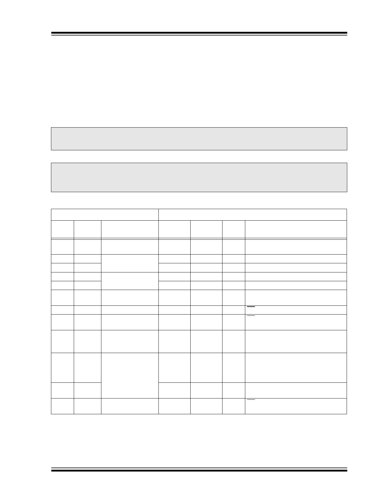
TABLE 1-1: DC CHARACTERISTICS
DC CHARACTERISTICS
Extended (H): TA = -40°C to +150°C
VCC = 2.5V to 5.5V
Param.
No.
Sym.
Characteristic
Min.
Max. Units
Test Conditions
D001 VIH1
D002 VIL1
D003 VIL2
D004 VOL
D005 VOL
D006 VOH
D007 ILI
D008 ILO
High-level input
voltage
Low-level input
voltage
Low-level output
voltage
High-level output
voltage
Input leakage current
Output leakage
current
.7 VCC
-0.3
-0.3
—
—
VCC -0.5
—
—
VCC+1
0.3VCC
0.2VCC
0.4
0.2
—
±2
±2
V
V VCC ≥ 2.7V
V VCC < 2.7V
V IOL = 2.1 mA
V IOL = 1.0 mA
V IOH = -400 μA
μA CS = VCC, VIN = VSS OR VCC
μA CS = VCC, VOUT = VSS OR VCC
D009 CINT
Internal Capacitance
—
(all inputs and
outputs)
7
pF TA = 25°C, CLK = 1.0 MHz,
VCC = 5.0V (Note)
D010 ICC Read
—
—
Operating Current
5
mA
2.5
mA
D011 ICC Write
—
5
mA
—
3
mA
D012 ICCS
Standby Current
—
10
μA
—
Note: This parameter is periodically sampled and not 100% tested.
VCC = 5.5V; FCLK = 5.0 MHz;
SO = Open
VCC = 2.5V; FCLK = 3.0 MHz;
SO = Open
VCC = 5.5V
VCC = 2.5V
CS = VCC = 5.5V, Inputs tied to VCC or
VSS, 150°C
© 2009 Microchip Technology Inc.
Preliminary
DS22136B-page 3
Share Link: 