25LC010A データシートの表示(PDF) - Microchip Technology
部品番号
コンポーネント説明
メーカー
25LC010A Datasheet PDF : 24 Pages
| |||
25LCXXXA
3.0 FUNCTIONAL DESCRIPTION
3.1 Principles of Operation
The 25LCXXXA are low-density serial EEPROMs
designed to interface directly with the Serial Peripheral
Interface (SPI) port of many of today’s popular micro-
controller families, including Microchip’s PIC® micro-
controllers. It may also interface with microcontrollers
that do not have a built-in SPI port by using discrete I/
O lines programmed properly in firmware to match the
SPI protocol.
The 25LCXXXA contains an 8-bit instruction register.
The device is accessed via the SI pin, with data being
clocked in on the rising edge of SCK. The CS pin must
be low and the HOLD pin must be high for the entire
operation.
Table 3-1 contains a list of the possible instruction
bytes and format for device operation. All instructions,
addresses, and data are transferred MSB first, LSB
last.
Data (SI) is sampled on the first rising edge of SCK
after CS goes low. If the clock line is shared with other
peripheral devices on the SPI bus, the user can assert
the HOLD input and place the 25LCXXXA in ‘HOLD’
mode. After releasing the HOLD pin, operation will
resume from the point when the HOLD was asserted.
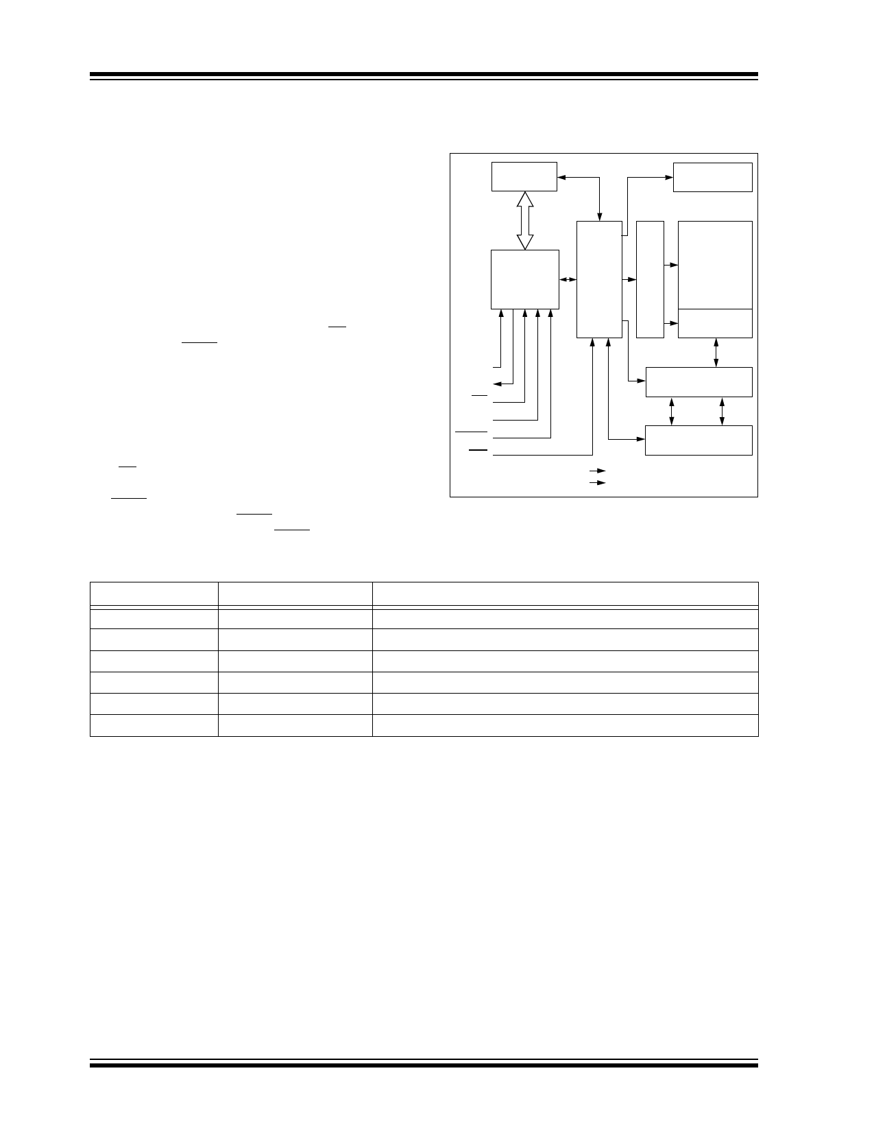
BLOCK DIAGRAM
STATUS
Register
HV Generator
I/O Control
Logic
Memory X
Control
Logic Dec
EEPROM
Array
Page Latches
SI
SO
CS
SCK
HOLD
WP
VCC
VSS
Y Decoder
Sense Amp.
R/W Control
TABLE 3-1: INSTRUCTION SET
Instruction Name Instruction Format
Description
READ
WRITE
WRDI
0000 A8011
0000 A8010
0000 x100
Read data from memory array beginning at selected address
Write data to memory array beginning at selected address
Reset the write enable latch (disable write operations)
WREN
0000 x110
Set the write enable latch (enable write operations)
RDSR
0000 x101
Read STATUS register
WRSR
0000 x001
Write STATUS register
Note: For the 24LC040A device, A8 is the 9th address bit, which is used to address the entire 512 byte array.
For the 24LC020A and 24LC010A devcies, A8 is a don’t care.
x = don’t care.
DS22136B-page 8
Preliminary
© 2009 Microchip Technology Inc.
Share Link: 