25AA080C データシートの表示(PDF) - Microchip Technology
部品番号
コンポーネント説明
メーカー
25AA080C Datasheet PDF : 28 Pages
| |||
25XX080C/D
2.5 Read Status Register (RDSR)
Instruction
The Read Status Register (RDSR) instruction provides
access to the STATUS register. The STATUS register
may be read at any time, even during a write cycle. The
STATUS register is formatted as follows:
TABLE 2-2: STATUS REGISTER
7
654 3
2
1
0
W/R – – – W/R W/R R
R
WPEN X X X BP1 BP0 WEL WIP
W/R = writable/readable. R = read-only.
The Write-In-Process (WIP) bit indicates whether the
25XX080C/D is busy with a write operation. When set
to a ‘1’, a write is in progress, when set to a ‘0’, no write
is in progress. This bit is read-only.
The Write Enable Latch (WEL) bit indicates the status
of the write enable latch and is read only. When set to
a ‘1’, the latch allows writes to the array or the STATUS
register, when set to a ‘0’, the latch prohibits writes to
the array or the STATUS register. The state of this bit
can always be updated via the WREN or WRDI com-
mands regardless of the state of write protection on the
STATUS register. These commands are shown in
Figure 2-4 and Figure 2-5.
The Block Protection (BP0 and BP1) bits indicate
which blocks are currently write-protected. These bits
are set by the user issuing the WRSR instruction, which
is in Figure 2-7. These bits are nonvolatile and are
shown in Table 2-3.
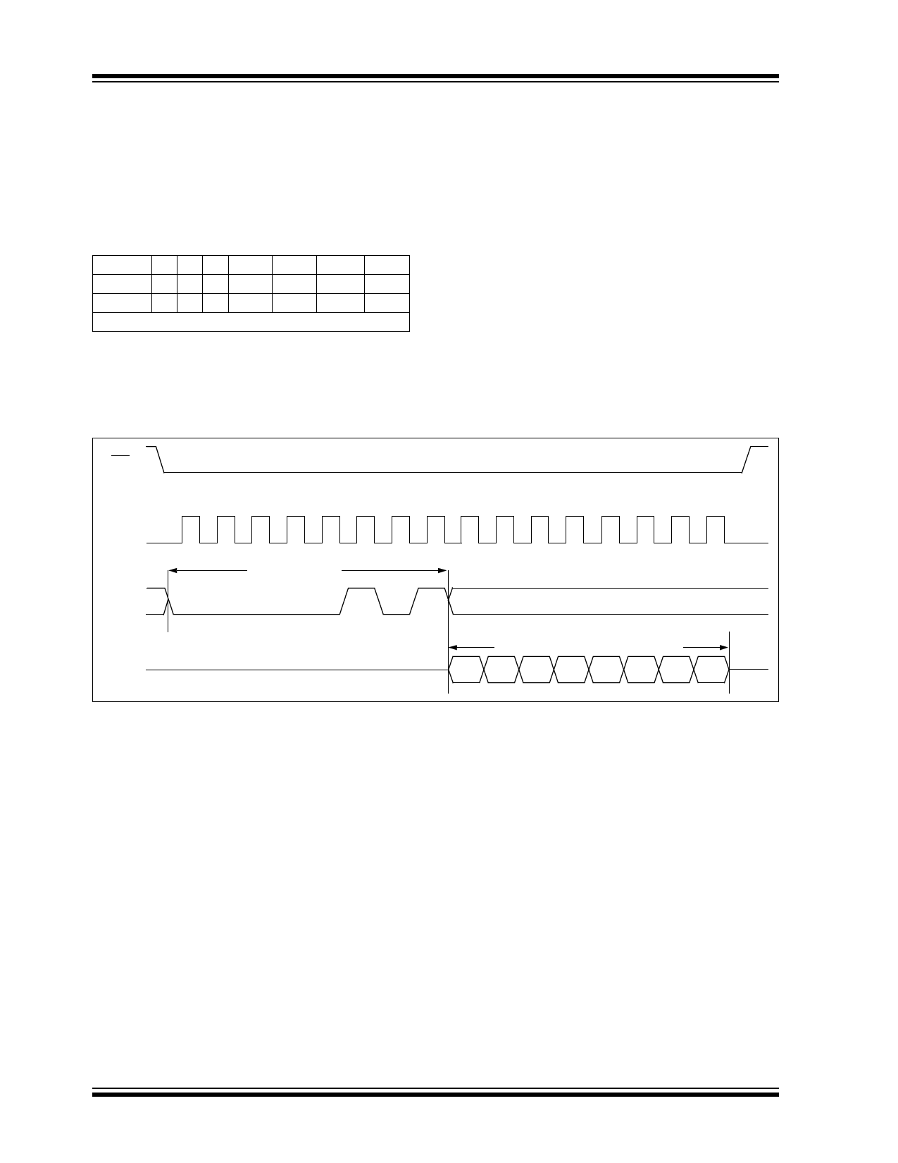
See Figure 2-6 for the RDSR timing sequence.
FIGURE 2-6: READ STATUS REGISTER TIMING SEQUENCE (RDSR)
CS
SCK
SI
SO
0 1 2 3 4 5 6 7 8 9 10 11 12 13 14 15
Instruction
0 00 00 1 01
High-Impedance
Data from STATUS Register
7 6 54 3 2 10
DS22151A-page 10
© 2009 Microchip Technology Inc.
Share Link: 