LCX026BLT データシートの表示(PDF) - Sony Semiconductor
部品番号
コンポーネント説明
メーカー
LCX026BLT Datasheet PDF : 25 Pages
| |||
LCX026BLT
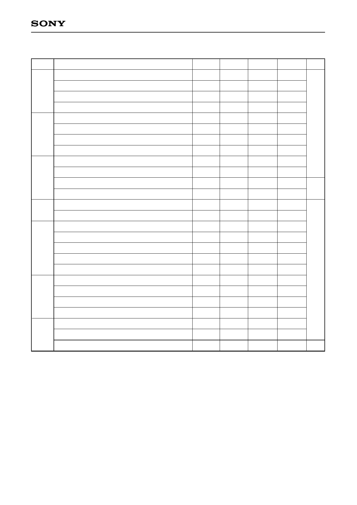
2. Clock timing conditions (Ta = 25°C)
(SVGA mode: fHCKn = 4.0MHz, fVCK = 24.0kHz)
Item
Symbol Min.
Typ.
Max. Unit
HST
HCK
VST
Hst rise time
Hst fall time
Hst data set-up time
Hst data hold time
Hckn rise time∗4
Hckn fall time∗4
Hck1 fall to Hck2 rise time
Hck1 rise to Hck2 fall time
Vst rise time
Vst fall time
Vst data set-up time
Vst data hold time
trHst
—
—
30
tfHst
—
—
30
tdHst
50
60
70
thHst
50
60
70
trHckn
—
—
30
ns
tfHckn
—
—
30
to1Hck –15
0
15
to2Hck –15
0
15
trVst
—
—
100
tfVst
—
—
100
tdVst
5
thVst
5
10
15
µs
10
15
Vck rise time
VCK
Vck fall time
trVck
—
tfVck
—
—
100
—
100
Enb rise time
trEnb
—
—
100
Enb fall time
tfEnb
—
—
100
ENB Vck rise/fall to Enb rise time
toEnb
400
500
—
Horizontal video period completed to Enb fall time tdEnb
900
1000
Enb fall to Pcg rise time
toPcg
630
700
—
—
ns
Pcg rise time
trPcg
—
—
30
Pcg fall time
PCG
Pcg rise to Vck rise/fall time
tfPcg
—
—
30
toVck
0
1000
1100
Pcg pulse width
twPcg 1100
1200
1300
Blk rise time
BLK∗5 Blk fall time
trBlk
—
—
100
tfBlk
—
—
100
Blk fall to Vst rise time
toVst
32
33
34
µs
∗4 Hckn means Hck1 and Hck2.
∗5 Blk is set to positive polarity pulse for other than SVGA mode ; Low level for SVGA mode.
–7–
Share Link: 