LCX026BLT データシートの表示(PDF) - Sony Semiconductor
部品番号
コンポーネント説明
メーカー
LCX026BLT Datasheet PDF : 25 Pages
| |||
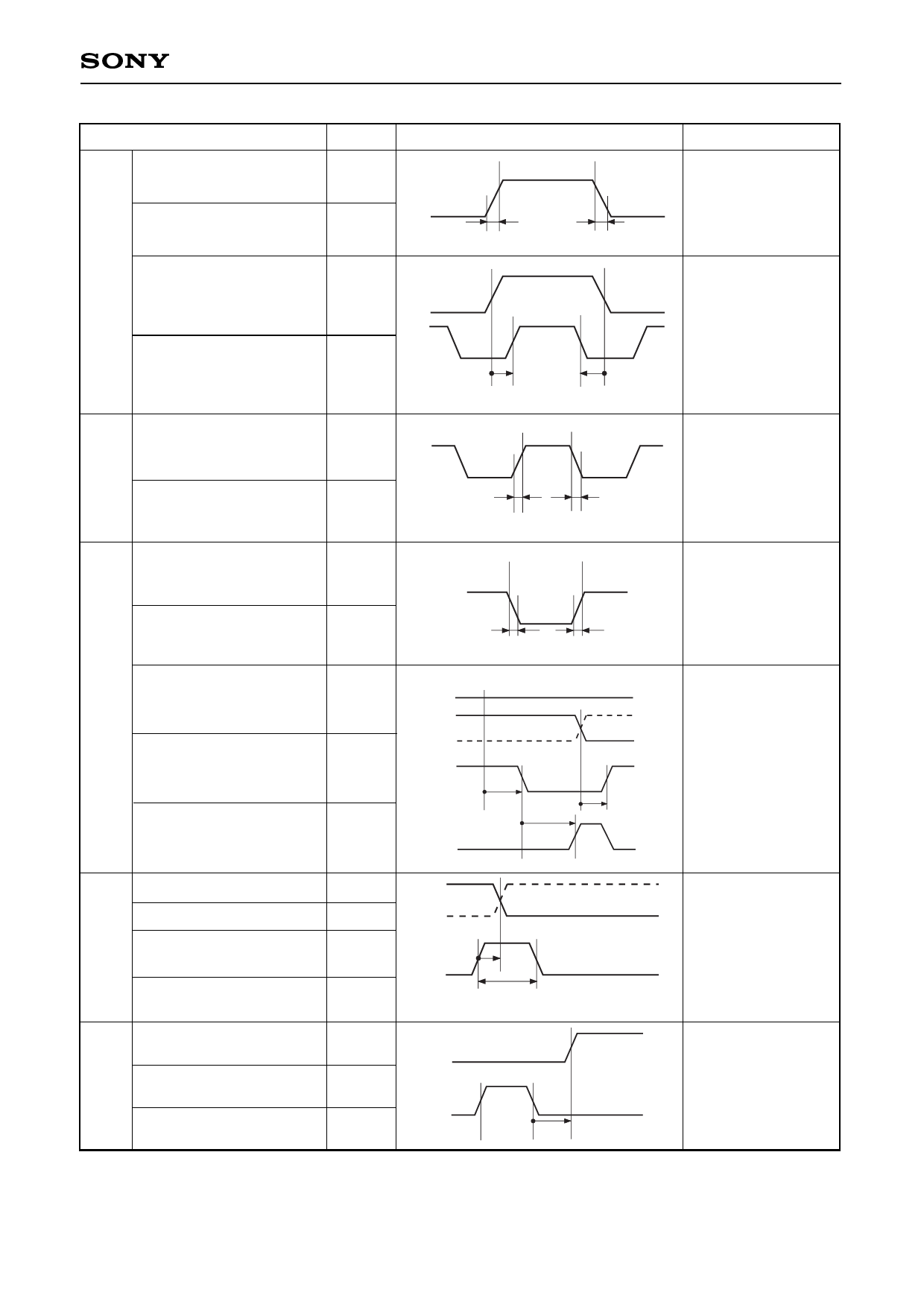
<Vertical Shift Register Driving Waveform>
Item
Symbol
Waveform
Vst rise time
Vst fall time
VST
Vst data set-up time
trVst
tfVst
tdVst
90%
Vst 10%
trVst
∗6
50%
Vst
50%
90%
10%
tfVst
50%
50%
Vst data hold time
Vck rise time
VCK
Vck fall time
thVst
trVck
tfVck
Vck
tdVst
90%
10%
Vck
thVst
90%
10%
trVckn tfVckn
LCX026BLT
Conditions
Enb rise time
trEnb
Enb fall time
tfEnb
Vck rise/fall to Enb rise
ENB time
toEnb
Horizontal video period
completed to Enb fall time
tdEnb
Enb fall to Pcg rise time toPcg
Pcg rise time
Pcg fall time
PCG∗7 Pcg rise to Vck rise/fall
time
Pcg pulse width
Blk rise time
trPcg
tfPcg
toVck
trPcg
twBlk
90%
90%
10% 10%
Enb
tfEn
trEn
Horizontal
video period
Horizontal blanking period
Vck
50%
Enb
toEnb 50%
50%
toPcg tdEnb
50%
Pcg
∗6
Vck
50%
toVck
50%
50%
Pcg
twPcg
∗6
Vst
50%
BLK Blk fall time
tfBlk
Blk 50%
50%
Blk fall to Vst rise time
toVst
∗6
toVst
∗7 Input the pulse obtained by taking the OR of the above pulse (PCG) and BLK to the PCG input pin.
–9–
Share Link: 