2N6660(2001) データシートの表示(PDF) - Vishay Semiconductors
部品番号
コンポーネント説明
メーカー
2N6660 Datasheet PDF : 4 Pages
| |||
2N6660, VQ1004J/P
Vishay Siliconix
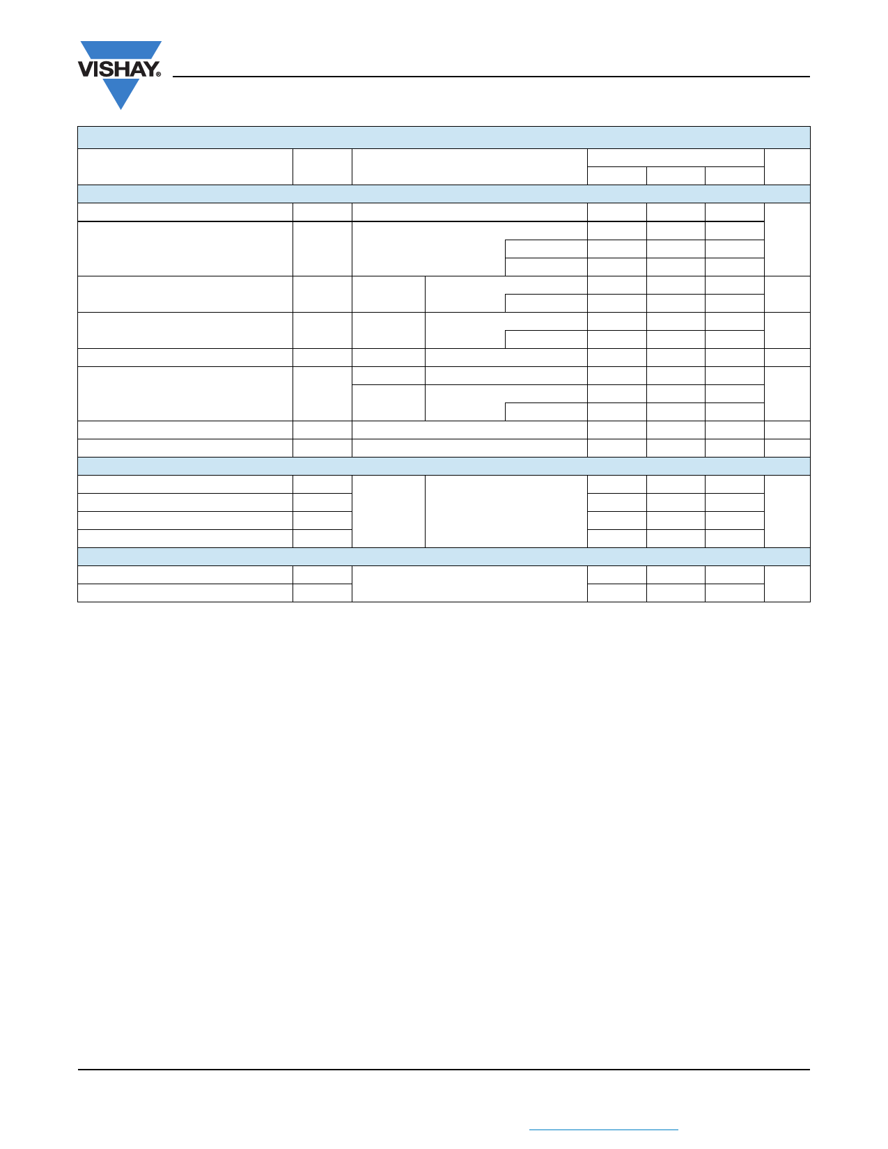
SPECIFICATIONS (TA = 25_C UNLESS OTHERWISE NOTED)
Parameter
Symbol
Test Conditions
Static
Drain-Source
Breakdown Voltage
Gate-Threshold Voltage
Gate-Body Leakage
Zero Gate
Voltage Drain Current
On-State Drain Currentb
Drain-Source On-Resistanceb
Forward Transconductanceb
Common Source
Output Conductanceb
Diode Forward Voltage
Dynamic
V(BR)DSS
VGS(th)
IGSS
IDSS
ID(on)
rDS(on)
gfs
gos
VSD
VGS = 0 V, ID = 10 mA
VDS = VGS, ID = 1 mA
VDS = 0 V, VGS = "15 V
TC = 125_C
VDS = 60 V, VGS = 0 V
VDS = 35 V, VGS = 0 V
VDS = 48 V, VGS = 0 V
TC = 125_C
VDS = 28 V, VGS = 0 V
TC = 125_C
VDS = 10 V, VGS = 10 V
VGS = 5 V, ID = 0.3 Ad
VGS = 10 V, ID = 1 A
TC = 125_Cd
VDS = 10 V, ID = 0.5 A
VDS = 10 V, ID = 0.1 A
IS = 0.99 A, VGS = 0 V
Input Capacitance
Output Capacitance
Reverse Transfer Capacitance
Drain-Source Capacitance
Switchingc
Ciss
Coss
Crss
Cds
VDS = 24 V, VGS = 0 V
f = 1 MHz
Turn-On Time
Turn-Off Time
tON
tOFF
VDD = 25 V, RL = 23 W
ID ^ 1 A, VGEN = 10 V
RG = 25 W
Notes
a. For DESIGN AID ONLY, not subject to production testing.
b. Pulse test: PW v80 ms duty cycle v1%.
c. Switching time is essentially independent of operating temperature.
d. This parameter not registered with JEDEC on 2N6660.
Typa
75
1.7
3
2
1.3
2.4
350
1
0.8
35
25
7
30
8
8.5
Limits
2N6660
VQ1004J/P
Min Max Min Max
Unit
60
60
V
0.8
2
0.8
2.5
"100
"500
"100
nA
"500
10
1
mA
500
500
1.5
1.5
A
5
5
3
3.5
W
4.2
4.9
170
170
mS
V
50
60
40
50
pF
10
10
40
10
10
ns
10
10
VNDQ06
www.vishay.com
11-2
Document Number: 70222
S-04379—Rev. E, 16-Jul-01
Share Link: 