AV16541DL データシートの表示(PDF) - Philips Electronics
部品番号
コンポーネント説明
メーカー
AV16541DL Datasheet PDF : 10 Pages
| |||
Philips Semiconductors
2.5V/3.3V 16-bit buffer/driver (3-State)
Product specification
74ALVT16541
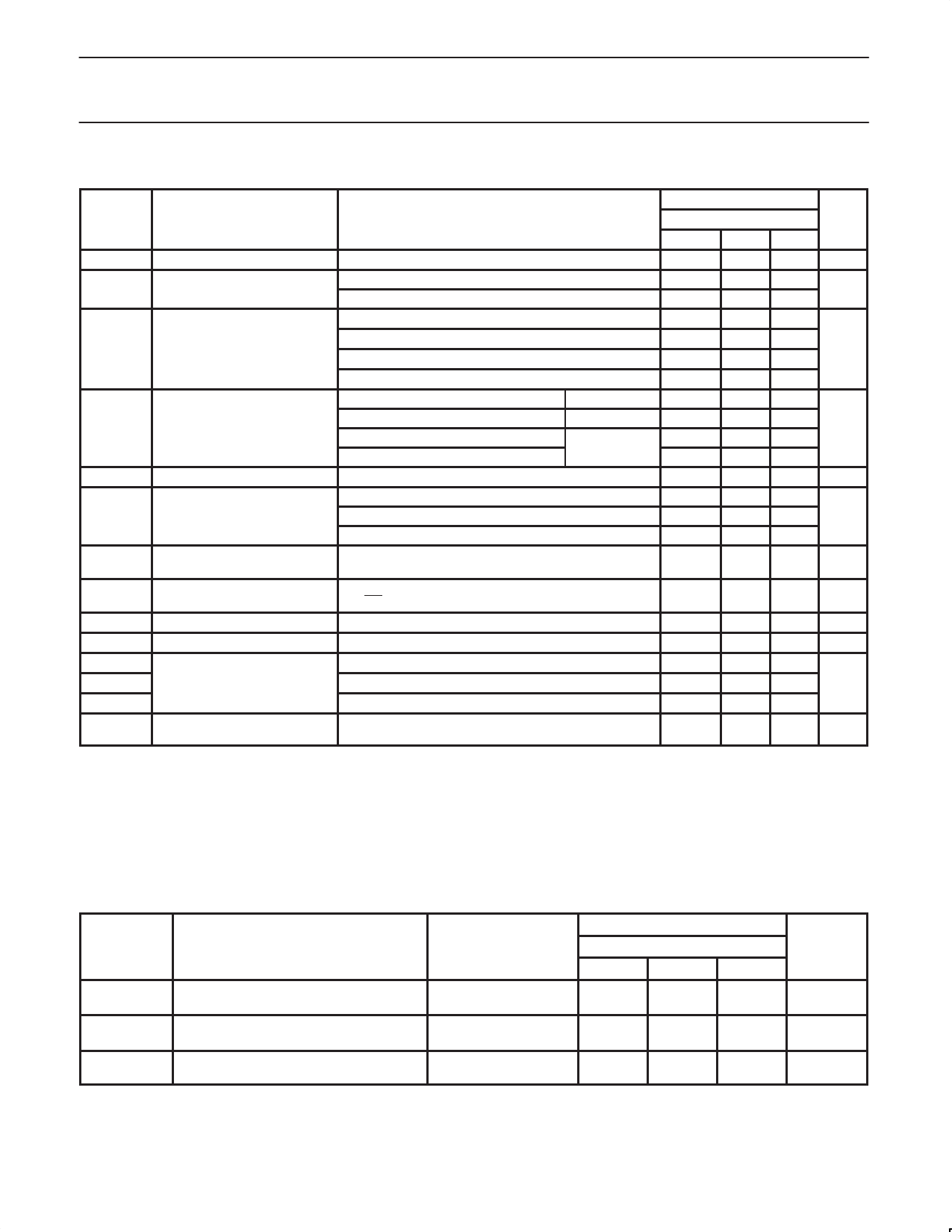
DC ELECTRICAL CHARACTERISTICS (3.3V "0.3V RANGE)
LIMITS
SYMBOL
PARAMETER
TEST CONDITIONS
Temp = -40°C to +85°C UNIT
MIN TYP1 MAX
VIK
Input clamp voltage
VCC = 3.0V; IIK = –18mA
–0.85 –1.2
V
VOH
High-level output voltage
VCC = 3.0 to 3.6V; IOH = –100µA
VCC = 3.0V; IOH = –32mA
VCC–0.2 VCC
V
2.0
2.3
VCC = 3.0V; IOL = 100µA
0.07 0.2
VOL
Low–level output voltage
VCC = 3.0V; IOL = 16mA
0.25 0.4
V
VCC = 3.0V; IOL = 32mA
0.3 0.5
VCC = 3.0V; IOL = 64mA
0.4 0.55
VCC = 3.6V; VI = VCC or GND
Control pins
0.1
±1
II
Input leakage current
VCC = 0 or 3.6V; VI = 5.5V
VCC = 3.6V; VI = VCC
VCC = 3.6V; VI = 0V
Data pins4
0.1
10
µA
0.5
1
0.1
-5
IOFF
Off current
VCC = 0V; VI or VO = 0 to 4.5V
0.1 ±100 µA
IHOLD
Bus Hold current
Data inputs6
VCC = 3V; VI = 0.8V
VCC = 3V; VI = 2.0V
VCC = 0V to 3.6V; VCC = 3.6V
75
130
–75 –140
µA
±500
IEX
Current into an output in the
High state when VO > VCC
VO = 5.5V; VCC = 3.0V
50
125
µA
IPU/PD
Power up/down 3-State output VCC ≤ 1.2V; VO = 0.5V to VCC; VI = GND or VCC;
current3
OE/OE = Don’t care
40 ±100 µA
IOZH 3-State output High current
VCC = 3.6V; VO = 3.0V; VI = VIL or VIH
0.5
5
µA
IOZL
3-State output Low current
VCC = 3.6V; VO = 0.5V; VI = VIL or VIH
0.5
–5
µA
ICCH
VCC = 3.6V; Outputs High, VI = GND or VCC, IO = 0
0.07 0.1
ICCL
Quiescent supply current
VCC = 3.6V; Outputs Low, VI = GND or VCC, IO = 0
3.2
5
mA
ICCZ
VCC = 3.6V; Outputs Disabled; VI = GND or VCC, IO = 05
0.07 0.1
∆ICC
Additional supply current per
input pin2
VCC = 3V to 3.6V; One input at VCC–0.6V,
Other inputs at VCC or GND
0.04 0.4 mA
NOTES:
1. All typical values are at VCC = 3.3V and Tamb = 25°C.
2. This is the increase in supply current for each input at the specified voltage level other than VCC or GND
3. This parameter is valid for any VCC between 0V and 1.2V with a transition time of up to 10msec. From VCC = 1.2V to VCC = 3.3V ± 0.3V a
transition time of 100µsec is permitted. This parameter is valid for Tamb = 25°C only.
4. Unused pins at VCC or GND.
5. ICCZ is measured with outputs pulled up to VCC or pulled down to ground.
6. This is the bus hold overdrive current required to force the input to the opposite logic state.
AC CHARACTERISTICS (3.3V "0.3V RANGE)
GND = 0V; tR = tF = 2.5ns; CL = 50pF; RL = 500Ω; Tamb = –40°C to +85°C.
SYMBOL
PARAMETER
WAVEFORM
tPLH
Propagation delay
tPHL
nAx to nYx
1
tPZH
Output enable time
tPZL
to High and Low level
2
tPHZ
Output disable time
tPLZ
from High and Low Level
2
NOTE:
1. All typical values are at VCC = 3.3V and Tamb = 25°C.
LIMITS
VCC = 3.3V "0.3V
MIN
TYP1
MAX
0.5
1.4
2.3
0.5
1.4
2.3
1.0
3.0
4.8
1.0
2.3
3.7
1.5
3.3
4.7
1.5
2.8
3.9
UNIT
ns
ns
ns
1998 Feb 13
5
Share Link: 