3D3522M-5 データシートの表示(PDF) - Data Delay Devices
部品番号
コンポーネント説明
メーカー
3D3522M-5 Datasheet PDF : 4 Pages
| |||
DEVICE SPECIFICATIONS
3D3522
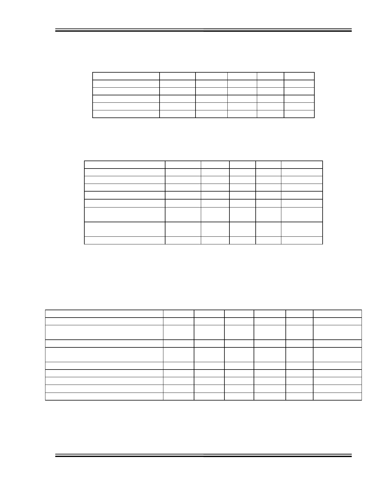
TABLE 2: ABSOLUTE MAXIMUM RATINGS
PARAMETER
SYMBOL MIN
MAX UNITS NOTES
DC Supply Voltage
Input Pin Voltage
Input Pin Current
Storage Temperature
Lead Temperature
VDD
VIN
IIN
TSTRG
TLEAD
-0.3
7.0
V
-0.3
VDD+0.3
V
-10
10
mA
25C
-55
150
C
300
C
10 sec
TABLE 3: DC ELECTRICAL CHARACTERISTICS
(-40C to 85C, 3.0V to 3.6V)
PARAMETER
Static Supply Current*
High Level Input Voltage
Low Level Input Voltage
High Level Input Current
Low Level Input Current
High Level Output Current
SYMBOL
IDD
VIH
VIL
IIH
IIL
IOH
Low Level Output Current
IOL
Output Rise & Fall Time
TR & TF
*IDD(Dynamic) = 2 * CLD * VDD * F
where: CLD = Average capacitance load/pin (pf)
F = Input frequency (GHz)
MIN MAX UNITS NOTES
5
mA
2.0
V
1.0
V
1.0
µA
VIH = VDD
1.0
µA
VIL = 0V
-4.0
mA VDD = 3.0V
VOH = 2.4V
4.0
mA VDD = 3.0V
VOL = 0.4V
2
ns
CLD = 5 pf
Input Capacitance = 10 pf typical
Output Load Capacitance (CLD) = 25 pf max
TABLE 4: AC ELECTRICAL CHARACTERISTICS
(-40C to 85C, 3.0V to 3.6V, except as noted)
PARAMETER
Nominal Input Baud Rate
Allowed Input Baud Rate Deviation
SYMBOL
fBN
fB
MIN
5
-0.15 fBN
TYP
MAX
50
0.15 fBN
UNITS
MBaud
MBaud
Allowed Input Baud Rate Deviation
Allowed Input Baud Rate Deviation
fB
-0.05 fBN
fB
-0.03 fBN
0.05 fBN MBaud
0.03 fBN MBaud
Allowed Input Duty Cycle
42.5
50.0
57.5
%
Bit Cell Time
tc
1000/fB
ns
Input Data Edge to Clock Falling Edge
tCL
0.75 tc
ns
Clock Width Low
tCWL
500/fBN
ns
Clock Falling Edge to Data Transition
tCD
3.0
4.0
5.0
ns
NOTES
0C to 70C
25C, 3.3V
3.0V to 3.6V
-55C to 125C
3.0V to 3.6V
±2ns or 5%
Doc #06005
DATA DELAY DEVICES, INC.
3
5/8/2006
3 Mt. Prospect Ave. Clifton, NJ 07013
Share Link: 