4N45 データシートの表示(PDF) - HP => Agilent Technologies
部品番号
コンポーネント説明
メーカー
4N45 Datasheet PDF : 7 Pages
| |||
Package Characteristics
For 0°C ≤ TA ≤ 70°C, unless otherwise specified. All typicals at TA = 25°C.
Parameter
Symbol Min. Typ. Max. Units Test Conditions
Input-Output Momentary
Withstand Voltage*
VISO 2500
Resistance, Input-Output RI-O
1012
Capacitance, Input-Output CI-O
0.6
V rms
Ω
pF
RH ≤ 50%, t = 1 min,
TA = 25°C
VI-O = 500 Vdc
f = 1 MHz
Fig. Notes
7, 10
7
7
*The Input-Output Momentary Withstand Voltage is a dielectric voltage rating that should not be interpreted as an input-output
continuous voltage rating. For the continuous voltage rating refer to the VDE 0884 Insulation Characteristics Table (if applicable),
your equipment level safety specification, or HP Application Note 1074, “Optocoupler Input-Output Endurance Voltage.”
Notes:
1. Derate linearly above 50°C free-air
temperature at a rate of 0.4 mA/°C.
2. Derate linearly above 50°C free-air
temperature at a rate of 0.7 mW/°C.
3. Derate linearly above 25°C free-air
temperature at a rate of 0.8 mA/°C.
4. Derate linearly above 25°C free-air
temperature at a rate of 1.5 mW/°C.
5. DC CURRENT TRANSFER RATIO is
defined as the ratio of output
collector current, IO, to the forward
LED input current, IF, times 100%.
6. Pin 6 Open.
7. Device considered a two-terminal
device: Pins 1, 2, 3 shorted together
and Pins 4, 5, and 6 shorted together.
8. Use of a resistor between pin 4 and 6
will decrease gain and delay time.
(See Figures 11, 12, and 13.)
9. Common mode transient immunity in
Logic High level is the maximum
tolerable (positive) dVcm/dt on the
leading edge of the common mode
pulse, VCM, to assure that the output
will remain in a Logic High state (i.e.,
VO > 2.5 V). Common mode transient
immunity in Logic Low level is the
maximum tolerable (negative)
dVcm/dt on the trailing edge of the
common mode pulse signal, Vcm, to
assure that the output will remain in
a Logic Low state (i.e., VO < 2.5 V).
10. In accordance with UL 1577, each
optocoupler is proof tested by
applying an insulation test voltage
≥ 3000 V rms for 1 second (leakage
detection current limit, II-O ≤ 5 µA).
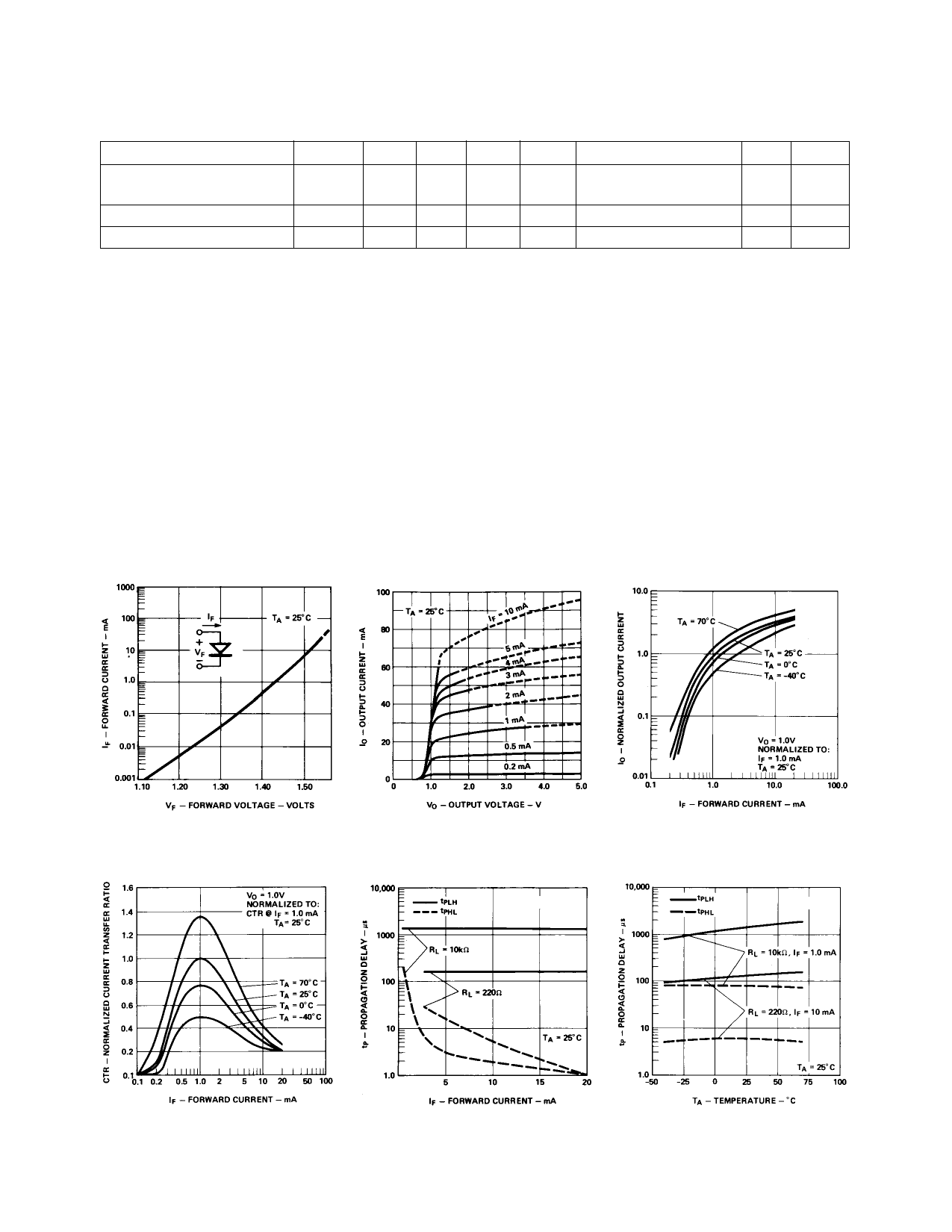
Figure 2. Input Diode Forward
Current vs. Forward Voltage.
Figure 3. Typical DC Transfer
Characteristics.
VCC = 5 V
Figure 4. Output Current vs. Input
Current.
VCC = 5 V
Figure 5. Current Transfer Ratio vs.
Input Current.
1-438
Figure 6. Propagation Delay vs.
Forward Current.
Figure 7. Propagation Delay vs.
Temperature.
Share Link: 