DSP56F802TA80 データシートの表示(PDF) - Freescale Semiconductor
部品番号
コンポーネント説明
メーカー
DSP56F802TA80 Datasheet PDF : 40 Pages
| |||
Part 2 Signal/Connection Descriptions
2.1 Introduction
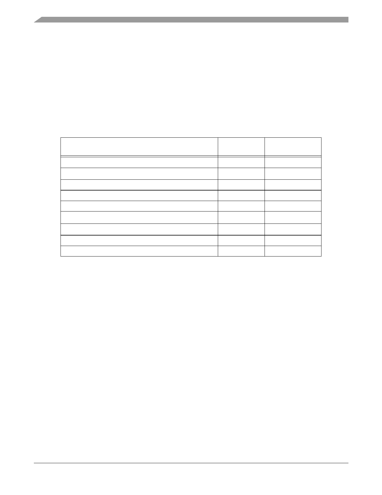
The input and output signals of the 56F802 are organized into functional groups, as shown in Table 2-1
and as illustrated in Figure 2-1. In Table 2-2 through Table 2-10, each table row describes the signal or
signals present on a pin.
Table 2-1 Functional Group Pin Allocations
Functional Group
Power (VDD or VDDA)
Ground (VSS, VSSA, TCS)
Supply Capacitors
Program Control
Pulse Width Modulator (PWM) Port and Fault Input
Serial Communications Interface (SCI) Port1
Analog-to-Digital Converter (ADC) Port (including VREF)
Quad Timer Module Port
JTAG/On-Chip Emulation (OnCE)
1. Alternately, GPIO pins
Number of
Pins
3
4
2
1
7
2
6
2
5
Detailed
Description
Table 2-2
Table 2-3
Table 2-4
Table 2-5
Table 2-6
Table 2-7
Table 2-8
Table 2-9
Table 2-10
56F802 Technical Data, Rev. 9
8
Freescale Semiconductor
Share Link: 