89C51 データシートの表示(PDF) - Philips Electronics
部品番号
コンポーネント説明
メーカー
89C51 Datasheet PDF : 32 Pages
| |||
Philips Semiconductors
80C51 8-bit microcontroller family
4K/8K/16K/32K Flash
Product specification
89C51/89C52/89C54/89C58
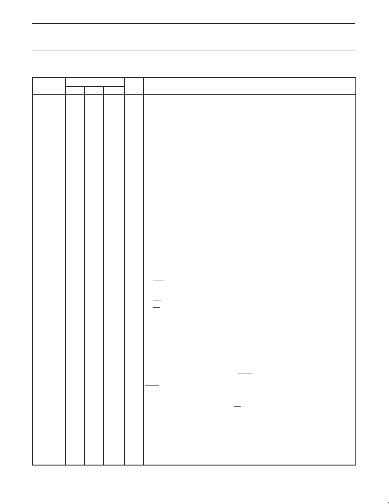
PIN DESCRIPTIONS
PIN NUMBER
MNEMONIC DIP LCC QFP TYPE NAME AND FUNCTION
VSS
VCC
P0.0–0.7
20
40
39–32
22
44
43–36
16
38
37–30
I Ground: 0 V reference.
I Power Supply: This is the power supply voltage for normal, idle, and power-down operation.
I/O Port 0: Port 0 is an open-drain, bidirectional I/O port. Port 0 pins that have 1s written to
them float and can be used as high-impedance inputs. Port 0 is also the multiplexed
low-order address and data bus during accesses to external program and data memory. In
this application, it uses strong internal pull-ups when emitting 1s.
P1.0–P1.7
1–8 2–9 40–44, I/O Port 1: Port 1 is an 8-bit bidirectional I/O port with internal pull-ups. Port 1 pins that have 1s
1–3
written to them are pulled high by the internal pull-ups and can be used as inputs. As inputs,
port 1 pins that are externally pulled low will source current because of the internal pull-ups.
(See DC Electrical Characteristics: IIL). Alternate function for Port 1:
1
2
40
I/O
T2 (P1.0): Timer/Counter2 external count input/clockout (see Programmable Clock-Out).
2
3
41
I
T2EX (P1.1): Timer/Counter2 reload/capture/direction control.
P2.0–P2.7
21–28 24–31 18–25
I/O Port 2: Port 2 is an 8-bit bidirectional I/O port with internal pull-ups. Port 2 pins that have 1s
written to them are pulled high by the internal pull-ups and can be used as inputs. As inputs,
port 2 pins that are externally being pulled low will source current because of the internal
pull-ups. (See DC Electrical Characteristics: IIL). Port 2 emits the high-order address byte
during fetches from external program memory and during accesses to external data memory
that use 16-bit addresses (MOVX @DPTR). In this application, it uses strong internal
pull-ups when emitting 1s. During accesses to external data memory that use 8-bit addresses
(MOV @Ri), port 2 emits the contents of the P2 special function register.
P3.0–P3.7 10–17 11,
5,
13–19 7–13
RST
ALE
10
11
5
11
13
7
12
14
8
13
15
9
14
16
10
15
17
11
16
18
12
17
19
13
9
10
4
30
33
27
PSEN
29
32
26
I/O Port 3: Port 3 is an 8-bit bidirectional I/O port with internal pull-ups. Port 3 pins that have 1s
written to them are pulled high by the internal pull-ups and can be used as inputs. As inputs,
port 3 pins that are externally being pulled low will source current because of the pull-ups.
(See DC Electrical Characteristics: IIL). Port 3 also serves the special features of the
89C51/89C52/89C54/89C58, as listed below:
I
RxD (P3.0): Serial input port
O
TxD (P3.1): Serial output port
I
INT0 (P3.2): External interrupt
I
INT1 (P3.3): External interrupt
I
T0 (P3.4): Timer 0 external input
I
T1 (P3.5): Timer 1 external input
O
WR (P3.6): External data memory write strobe
O
RD (P3.7): External data memory read strobe
I Reset: A high on this pin for two machine cycles while the oscillator is running, resets the
device. An internal diffused resistor to VSS permits a power-on reset using only an external
capacitor to VCC.
O Address Latch Enable: Output pulse for latching the low byte of the address during an
access to external memory. In normal operation, ALE is emitted at a constant rate of 1/6 the
oscillator frequency, and can be used for external timing or clocking. Note that one ALE
pulse is skipped during each access to external data memory. ALE can be disabled by
setting SFR auxiliary.0. With this bit set, ALE will be active only during a MOVX instruction.
O Program Store Enable: The read strobe to external program memory. When executing
code from the external program memory, PSEN is activated twice each machine cycle,
except that two PSEN activations are skipped during each access to external data memory.
PSEN is not activated during fetches from internal program memory.
EA/VPP
31
35
29
I External Access Enable/Programming Supply Voltage: EA must be externally held low
to enable the device to fetch code from external program memory locations 0000H to the
maximum internal memory boundary. If EA is held high, the device executes from internal
program memory unless the program counter contains an address greater than 0FFFH for
4 k devices, 1FFFH for 8 k devices, 3FFFH for 16 k devices, and 7FFFH for 32 k devices.
The value on the EA pin is latched when RST is released and any subsequent changes
have no effect. This pin also receives the 12.00 V programming supply voltage (VPP) during
FLASH programming.
XTAL1
19
21
15
I Crystal 1: Input to the inverting oscillator amplifier and input to the internal clock
generator circuits.
XTAL2
18
20
14
O Crystal 2: Output from the inverting oscillator amplifier.
NOTE: To avoid “latch-up” effect at power-on, the voltage on any pin (other than VPP) at any time must not be higher than VCC + 0.5 V or
VSS – 0.5 V, respectively.
1999 Oct 27
5
Share Link: 