RMWP23001 データシートの表示(PDF) - Raytheon Company
部品番号
コンポーネント説明
メーカー
RMWP23001 Datasheet PDF : 7 Pages
| |||
RMWP23001
21-24 GHz Power Amplifier MMIC
Application
Information
PRODUCT INFORMATION
CAUTION: THIS IS AN ESD SENSITIVE DEVICE.
Chip carrier material should be selected to have GaAs compatible thermal coefficient of expansion and high
thermal conductivity such as copper molybdenum or copper tungsten. The chip carrier should be machined,
finished flat, plated with gold over nickel and should be capable of withstanding 325°C for 15 minutes.
Die attachment should utilize Gold/Tin (80/20) eutectic alloy solder and should avoid hydrogen environment for
PHEMT devices. Note that the backside of the chip is gold plated and is used as RF and DC ground.
These GaAs devices should be handled with care and stored in dry nitrogen environment to prevent
contamination of bonding surfaces. These are ESD sensitive devices and should be handled with appropriate
precaution including the use of wrist grounding straps. All die attach and wire/ribbon bond equipment must be
well grounded to prevent static discharges through the device.
Recommended wire bonding uses 3 mils wide and 0.5 mil thick gold ribbon with lengths as short as practical
allowing for appropriate stress relief. The RF input and output bonds should be typically 0.012” long
corresponding to a typically 2 mil between the chip and the substrate material.
Recommended
Procedure
for Biasing and
Operation
CAUTION: LOSS OF GATE VOLTAGES (Vg) WHILE DRAIN VOLTAGES (Vd) IS PRESENT MAY DAMAGE THE
AMPLIFIER CHIP.
The following sequence of steps must be followed to properly test the amplifier.
Step 1: Turn off RF input power.
Step 2: Connect the DC supply grounds to the grounds
of the chip carrier. Slowly apply negative gate
bias supply voltage of -1.5 V to Vg.
Step 3: Slowly apply positive drain bias supply voltage
of +4 V to Vd.
Step 4: Adjust gate bias voltage to set the quiescent
current of Idq = 400 mA.
Step 5: After the bias condition is established, RF input
signal may now be applied at the appropriate
frequency band.
Step 6: Follow turn-off sequence of:
(i) Turn off RF input power,
(ii) Turn down and off drain voltage (Vd),
(iii) Turn down and off gate bias voltage (Vg).
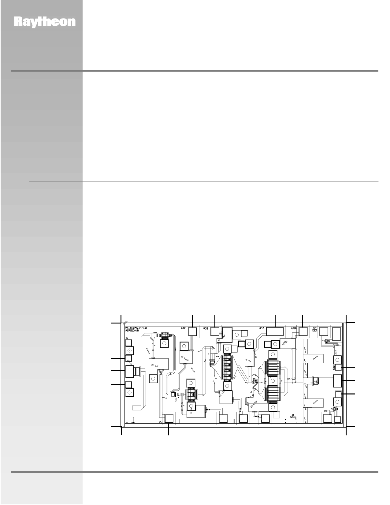
Chip Layout and
Bond Pad
Locations
Chip Layout and Bond
Pad Locations
Chip Size is 2.6 mm x
1.2 mm x 100 µm.
Back of chip is RF and
DC ground
Dimensions in mm
0.0
1.2
0.791
0.637
0.482
0.82 1.072
1.756
2.076
2.6
1.2
0.685
0.53
0.376
www.raytheon.com/micro
0.0
0.0
0.55
Characteristic performance data and specifications are subject to change without notice.
Revised March 14, 2001
Page 2
0.0
2.6
Raytheon RF Components
362 Lowell Street
Andover, MA 01810
Share Link: 