A1359 データシートの表示(PDF) - Allegro MicroSystems
部品番号
コンポーネント説明
メーカー
A1359 Datasheet PDF : 12 Pages
| |||
A1359
Factory-Programmed Dual Output Linear Hall Effect Sensor IC
With Analog and Pulse Width Modulated Outputs
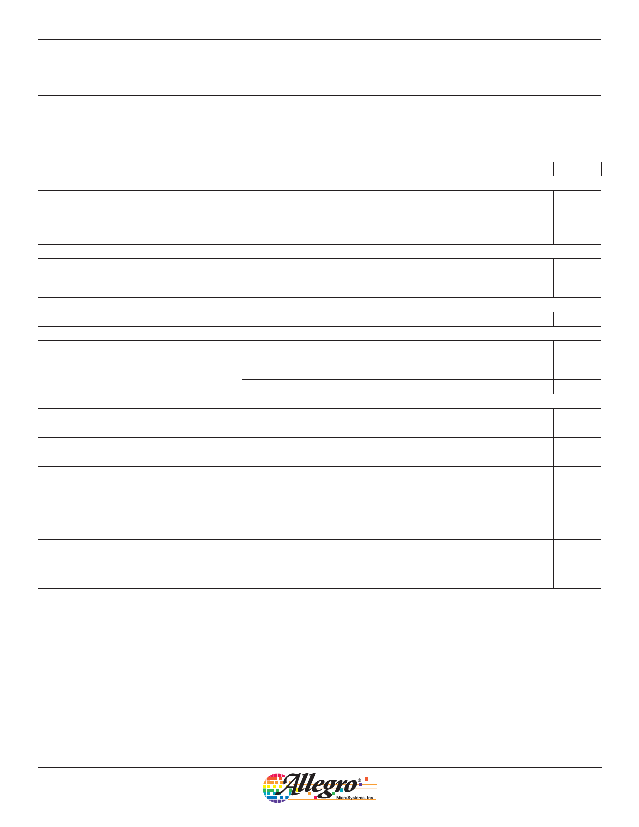
OPERATING CHARACTERISTICS (continued) Valid over full operating temperature range, TA, CBYPASS = 0.1 μF , VCC = 5 V,
unless otherwise noted
Characteristics
Symbol
Test Conditions
Min.
Typ.
Max.
Unit1
PWM Output Characteristics (continued)
Load Resistance3,6
Load Capacitance3,6
Duty Cycle Jitter3
RPULLUP PWMOUT to VCC
2000
–
–
Ω
CL
PWMOUT to GND
–
–
10
nF
JitterPWM
Measured over 1000 PWM output clock periods,
3 sigma values, Sens = 9 mV/G
–
±0.18
–
%D
Quiescent Voltage Output (QVO)
Quiescent Voltage Output
Quiescent Voltage Output
Equivalent PWM
VOUT(Q)
D(Q)
TA = 25°C
TA = 25°C, VCC = 4.5 to 5.5 V
2.45
2.5
2.55
V
49
50
51
%D
PWM Carrier Frequency
Carrier Frequency
Sensitivity
fPWM TA = 25°C
3.6
4
4.4
kHz
Sensitivity Temperature Coefficient
TCSENS
Programmed at TA = 150°C, calculated relative
to Sens at 25°C
0.08
0.12
0.16
%/°C
Analog Sensitivity7
Error Components
A1359LLETR-T
Sen
B = ±125 G, TA = 25°C
8.73
9.0
9.27
mV/G
A1359LLETR-RP-T B = ±125 G, TA = 25°C
–9.27
–9.0
–8.73
mV/G
PWM to Analog Output Mismatch8
VOUTERR
1.75 V < VOUT < 3.25 V
VOUT = 1.25 V, VOUT = 3.75 V
–57.4
–
+57.4
mV
–85
–
+85
mV
Linearity Sensitivity Error9
LinERR
–
±0.5
–
%
Symmetry Sensitivity Error9
SymERR
–
±0.5
–
%
Ratiometry Quiescent Voltage
Output Error10
RatVOUT(Q)
Across supply voltage range,
(relative to VCC = 5 V)
–
±0.5
–
%
Ratiometry Sensitivity Error9
RatSens
Across supply voltage range,
(relative to VCC = 5 V)
–
±0.5
–
%
Ratiometry Clamp Error10
RatVOUTCLP
TA = 25°C, across supply voltage range, (relative
to VCC = 5 V)
–
±0.5
–
%
Quiescent Voltage Output Drift Through
Temperature Range
∆VOUT(Q) TA =150°C
–17
–
+17
mV
Sensitivity Drift Due to Package
Hysteresis
∆SensPKG TA = 25°C, after temperature cycling
–
±2
–
%
11 G (gauss) = 0.1 mT (millitesla).
2At power-up, the output is held low until VCC exceeds VUVLOHI . When the device reaches the operational power level, the output remains valid until
VCC drops below VUVLOLO , when the output is pulled low.
3Determined by design and characterization, not evaluated at final test.
4fc varies as much as approximately ±20% across the full operating ambient temperature range and process.
5VCLPL and VCLPH scale with VCC , due to ratiometry.
6Load capacitance and resistance directly effects the rise time of the PWM output by tr = 0.35 × 2 × π × RL × CL.
7Room temperature sensitivity can drift, ΔSensLIFE , by an additional 3% (typical worst case) over the life of the product.
8See Characteristic Definitions section.
9Applicable to both analog and PWM channels. Tested at Allegro factory for only the analog channel, and determined by design and characterization
for the PWM channel.
10Applies only to the analog channel.
Allegro MicroSystems, Inc.
5
115 Northeast Cutoff
Worcester, Massachusetts 01615-0036 U.S.A.
1.508.853.5000; www.allegromicro.com
Share Link: 